Inside Boost
A gain knob for a quiet build · A TL072 on eight strips · By Onion Madder · Mess O' Pedals
Some builds come out too quiet. The Octave Avalanche is one, and there are others. This is a small board that goes inside one of them, between its circuit and its output, and makes it louder: one half of a TL072 with a gain knob from ×1 to about ×22, the other half holding a half-rail reference so it runs from the host's own supply. It has no jacks and no supply of its own. Four wires go to the host - supply, ground, in and out - and two to the knob.
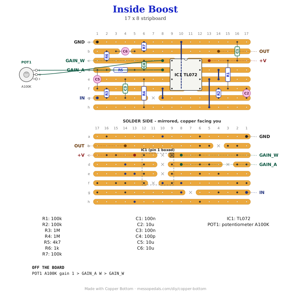
What you'll need
tap to expand / collapse
- 1× TL072 dual op-amp, 8-pin DIP (IC1) - spot it: TL072 on top, a notch or a dot marks pin 1. Socket it: an NE5532 sits in the same holes if you want to hear the difference
- 2× 1M resistor (R3, R4) - spot it: bands brown-black-green. R3 holds the input at ground and stands up; R4 biases the op-amp's input at the reference and lies across three holes
- 3× 100K resistor (R1, R2, R7) - spot it: bands brown-black-yellow. R1 and R2 are the half-rail divider. R7 holds the output at ground so it does not thump. R2 and R7 stand up
- 1× 4.7K resistor (R5) - spot it: bands yellow-violet-red. It sets the top of the gain: 1 plus 100K over 4.7K is about 22. It lies along its strip, over a cut
- 1× 1K resistor (R6) - spot it: bands brown-black-red. On the way out, so a long wire or a shorted jack cannot upset the chip. Stands up
- 1× 100n film capacitor (C3) - spot it: a small boxy cap marked 104 or 0.1. The input coupling cap. Ceramic works; film is quieter
- 1× 100n ceramic (C1) - spot it: 104. Across the chip's supply
- 1× 100p ceramic (C4) - spot it: 101. Across the feedback; it takes the fizz off the very top at full gain
- 3× 10 µF electrolytic (C2, C5, C6) - spot it: a small can with a stripe down one side; the stripe leg is the negative one. C2 holds the reference, C5 is in the gain leg, C6 is the output coupling cap. All three have their stripe toward ground or toward OUT: their plus sides sit at half the supply
- Stripboard, 8 strips × 17 holes or larger, and solid wire for four links, one of them under the chip
Off the board
- 1× A100K pot, the gain knob - spot it: the A on its back means log. Used as a variable resistor: lug 1 and the wiper, the third lug empty. A log pot puts noon at about ×3, where most of the useful range is; a B100K works and is crowded at the bottom. A 100K trimmer in the same two pads is the set-and-forget version
- Hookup wire for the four wires to the host. No supply and no power switch of its own: the host's switch is already upstream of +V
The layout file is the guide
Like the rest of the stripboard shelf, the build document for this one is the file itself: ↓ Download Inside_Boost.json - import it into Copper Bottom and the editor gives you the board picture, the placement walkthrough, the electrical checks and a printable build sheet, all from the same file. No coordinates are written out on this page on purpose: the editor is the viewer, and a number typed twice is a number that can drift.
One link runs under the chip. J1 goes straight down the column where the strips are cut, from the ground strip along the top to pin 4's strip, which is why pin 4's cut sits one hole further over than the others. Fit it before the socket. Pins 6 and 7 are tied together by J3 on purpose: that half of the chip is a follower.
The netlist
Quoted verbatim from the layout file. It was written from the board, so checking the board against it can only pass - what it is for is carrying the circuit somewhere else, and telling you what each strip is supposed to be doing while you stare at it.
The off-board wiring
Six pads leave the board. Four go to the host, two to the gain knob.
| Pad | Goes to |
|---|---|
| +V | The host's supply, after its power switch, so one switch turns both off. 9V is fine; anything up to 18V gives more room before it clips |
| GND | The host's ground |
| IN | The host's output: lift the wire that went from its board to its level pot or its output jack, and land it here instead. If the host has an output cap, keep it; this board has its own as well and does not mind two |
| OUT | Where that wire used to go: lug 3 of the host's level pot, or the output jack tip. With a level pot after it, the gain knob sets how hard it goes and the level pot sets how loud it comes out |
| GAIN_A | Gain pot, lug 1. The third lug stays empty |
| GAIN_W | Gain pot, wiper. All the way down is ×1, the host as it was; all the way up is about ×22 |
How it works, in one breath
An op-amp with feedback works to keep its two inputs at the same voltage. The signal goes into the plus input, and the output has to swing far enough that the slice of it coming back to the minus input matches. The gain pot and R5 are that slice: with the pot at zero the output is wired straight back and the stage is a follower, ×1; turned up to 100K, the output has to swing 1 plus 100K over 4.7K times as far, about ×22, or 27 dB. C5 in series with R5 means none of that applies to DC, so the output sits at the reference however the knob is set, and the knob has no DC across it to crackle.
The other half of the chip only holds a voltage. Two 100Ks split the supply in half, C2 steadies it, and op-amp B follows it, so the input is biased to a reference with an op-amp behind it. That is what lets it run from one 9V: the signal swings around four and a half volts, C3 keeps the host's DC out, and C6 keeps the four and a half volts in. Pins 6 and 7 tied together is the follower, not a mistake, if the checker mentions it.
Headroom, unmeasured. A TL072 is not a rail-to-rail chip: on 9V it swings about 6 volts peak to peak before it clips. A source that already comes out at a couple of volts reaches that at about ×3, and a square wave clipped mostly just gets squarer, so you may not hear it. If you do, run the board on 12V or more, or turn the gain down and let the host's own level pot do the rest.
Things to try
- Darker. C4 at 1n instead of 100p rolls the top off from about 1.6 kHz at full gain: a quick way to round off a fizzy square wave
- A fixed gain. Leave the pot off and put a resistor across GAIN_A and GAIN_W: 10K is about ×3, 22K about ×6, 47K about ×11
- A bypass. A DPDT that sends the host's signal either through the board or around it gives you before and after on one switch
- A different chip. Anything with the dual op-amp pinout drops into the socket. An NE5532 is quieter and swings a little further; an LM358 runs lower but sounds rougher at the top
The circuit is the single-supply non-inverting stage from every op-amp datasheet's application notes, with the reference buffered the way the Bug Mixer does it. The layout is Onion Madder's, drawn in Copper Bottom.