Cicada Rack
Four voices a clock can play · The Cicada NAND plus a rack block and four gate inputs · 12 HP · By Onion Madder · Mess O' Pedals
The Cicada NAND is four CD4093 oscillators with a pitch knob and a gate each - a toggle that lets the voice sing or holds it shut. In a rack a gate is something you patch, so this is that board with a gate jack for every voice: a clock, a sequencer or a square LFO plays the voices on and off, the toggles still kill one dead, and the four sum onto one output at rack level. One row of the panel per voice.
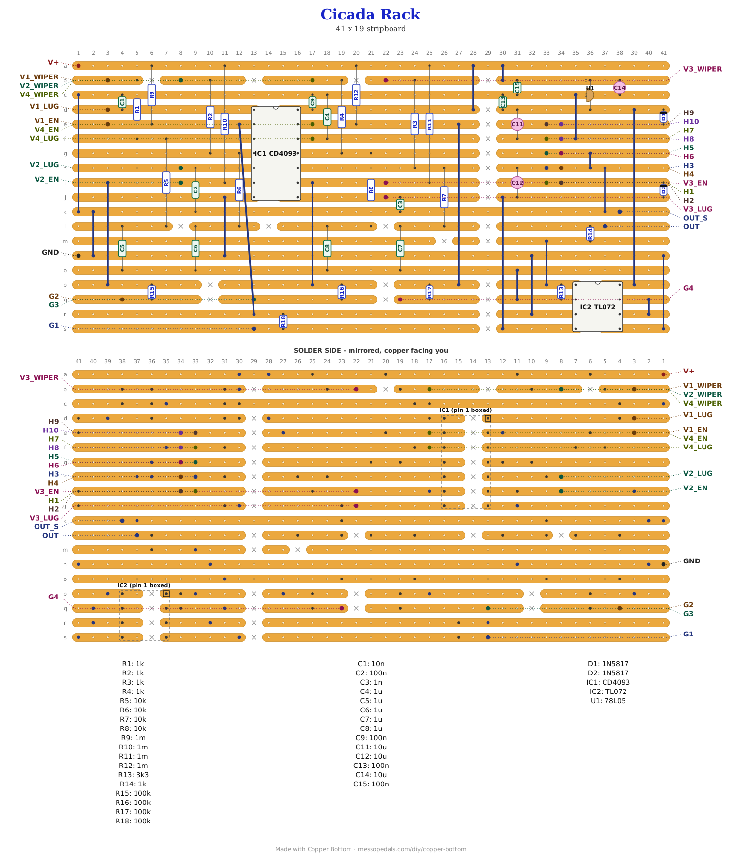
What you'll need
tap to expand / collapse
On the board, counted from the layout file:
- 1× CD4093 quad Schmitt NAND, 14-pin DIP (IC1)
- 1× TL072 dual op-amp, 8-pin DIP - spot it: TL072 printed on top, notch marks pin 1. An NE5532 or TL082 sits in the same holes (IC2)
- 4× 100k (brown-black-yellow; R15 to R18)
- 4× 10k (brown-black-orange; R5 to R8)
- 5× 1k (brown-black-red; R1 to R4, R14)
- 4× 1m (brown-black-green; R9 to R12)
- 1× 3k3 (orange-orange-red; R13)
- 4× 100n ceramic disc (104; C2, C9, C13, C15)
- 1× 10n ceramic disc (103; C1)
- 1× 1n ceramic disc (102; C3)
- 4× 1u film (105, or a small film cap; C5 to C8)
- 1× 1u ceramic disc (105, or a small film cap; C4)
- 3× 10u electrolytic (C11 to C12, C14) - spot it: the stripe marks the negative leg
- 2× 1N5817 Schottky, the reverse-polarity diode - spot it: a fat black body, band toward the cathode (D1 to D2)
- 1× 78L05 5 V regulator, TO-92 - spot it: 78L05 on the flat face; legs OUT, GND, IN with the flat face toward you (U1)
- 19 wire links (J1 to J4, J13 to J27) - solid core, tinned
- 1× 2×5 pin header, plain, 0.1″ - the Eurorack power connector. spot it: ten square pins in two rows. Not the shrouded kind; a shroud is 20 mm long and would cover the neighboring strips
- Stripboard, 19 strips × 41 holes or larger
Off the board
- 4× B1M 9 mm Alpha pots, the pitch knobs, wired as variable resistors, two lugs each, as the Cicada guide has them
- 4× SPST sub-mini toggles, the kill switches - one lug to a Vn_EN pad, the other to ground
- 5× Thonkiconn PJ398SM 3.5 mm jacks: four gates in, one out
- 1× 12 HP Eurorack blank panel, four knobs, and a Eurorack power cable
What is the Cicada, and what is new
Rows 0 to 14, columns 0 to 27 are Cicada_NAND.json hole for hole, and the script that
drew this re-derives every net of the Cicada from the new copper before it writes. Off came the
old 10 µF output cap and the two jack pads; the four 1 µF-and-10K legs still meet on
strip 14, the bus, and the bus now runs into the TL072's inverting input with 3K3 feedback -
one voice about ±0.8 V, four about ±3.3 V, out through 1K.
The gates. Each voice's EN pad still takes its toggle to ground, and the 1M pull-up still holds it high with nothing plugged, so a bare module drones on all four as before. The new gate jack reaches the same node through a 100K: a 0 V gate pulls it below the Schmitt threshold against the 1M, a +5 V gate lets it rise, and anything hotter or negative is clamped by the chip's own input diodes with the 100K holding the current to well under a tenth of a milliamp. The toggle still wins - it shorts the node - so it is a kill switch, and the jack plays.
Three of the four gate nodes ride down to the new strips under the board on links, and one cannot. V1_EN's segment has no free column beneath it, so J23 is a diagonal wire from (4,11) to (17,12) - a wire on the copper side, drawn as the slant it is, the same as the Bug Mixer's J4. Lay it on the solder side, or sleeve it.
The layout file is the guide
As on every stripboard guide here, the build document is the file itself: ↓ Download Cicada_Rack.json - import it into Copper Bottom and the editor gives you the board picture, the placement walkthrough, the electrical checks and a printable build sheet, all from the same file. No coordinates are written out on this page on purpose: the editor is the viewer, and a number typed twice is a number that can drift.
The netlist
Quoted verbatim from the layout file. It was written from the board, so checking the board against it can only pass - what it is for is carrying the circuit somewhere else, and telling you what each strip is supposed to be doing while you stare at it. The bug board's nets keep the names they have on its own page.
The off-board wiring
30 pads leave the board. Ten of them are the power header.
| Pad | Goes to |
|---|---|
| V1_LUG … V4_LUG, V1_WIPER … V4_WIPER | The four pitch pots, one LUG and one WIPER pad each, exactly as the Cicada guide wires them |
| V1_EN … V4_EN | The four kill toggles, one lug each; the other lug to ground. Open, the voice runs (or the jack decides); closed, it is dead |
| G1 … G4 | The four gate jacks, tips. Through 100K each onto the same node as the toggle. High plays the voice, low holds it |
| H1 … H10 | The power header, 2×5, pins down the strips. H1 and H2 are -12 V and take the cable's red stripe; H3 to H8 are ground; H9 and H10 are +12 V |
| OUT | The output jack, tip. The four voices, through the 1K |
| OUT_S | Every jack's sleeve, and the toggles' ground lugs |
| V+, GND | Test points: the 5 V rail and ground |
The panel
12 HP, which is 61.0 mm of a 128.5 mm blank - Amplified Parts sells reversible black-and-aluminum blanks in every width from 2 to 20 HP. The template is drawn for 9 mm Alpha pots (7 mm holes), Thonkiconn jacks (6 mm), sub-mini toggles (6.5 mm) and 5 mm LEDs, with the rack's rails kept clear top and bottom and the four M3 mounting holes where Doepfer puts them. I/O along the bottom, controls above, as everything on this site does it.
↓ cicada-rack-panel.pdf
Nobody has drilled this one yet - the holes are the module's pads, where they sit is the format applied to them.
The rack block, the same on every module
The right-hand end of every board on this shelf is the same idea drawn six times. The 2×5 header takes the rack's power cable, mounted with its pins running down the strips so each pair of pins lands on one strip: -12 V, then three grounds, then +12 V. That is the only way it can go on stripboard - turned the other way, the -12 and ground pins would share copper. The red stripe on the cable goes to H1 and H2. A 1N5817 stands in series with each rail so a cable put on backwards does nothing instead of everything. A 78L05 then makes a 5 V rail for the chip, and a TL072 on the real ±12 V does the rack-level work.
Five volts for the CMOS, not twelve, is what makes these rack-polite for free. A CD4000-series input switches near half its supply, so a +5 V gate from a sequencer clocks a 5 V chip directly but would never reach the ~7 V a 12 V chip wants; a pot across 5 V makes exactly the 0 to 5 V control voltage every rack sequencer speaks; and a hot or negative rack signal into a CMOS input needs only a 100K in series, the chip's own input diodes doing the clamping at well under a tenth of a milliamp. It is also a change from the 9 V these boards were built at - every chip is rated down to 3 V so the circuits are fine, but the oscillators will sit at slightly different pitches, and that is one of the things the bench is for.
The IDC socket on the power cable overhangs the header by about two strips at each end. Nothing tall stands there - the generator that drew this refuses to put anything standing under the socket - so keep it that way if you move a part.
How it works, in one breath
A 4093 gate is a 40106 inverter with a second input: hold that input high and the oscillator runs, pull it low and the output sits high and the cap stops charging. On the Cicada a toggle did the holding. Here a jack does it through a resistor big enough that the chip's own protection diodes can take whatever a rack throws at it, and small enough against the 1M pull-up that a low gate still wins. The summing stage is the Hive Rack's: the four voices push current into a virtual ground and the feedback resistor sets the size.
Things to try
- Patch the Firefly in. Its CLK OUT into a gate jack and one voice becomes a rhythm; its CV OUT does nothing here - the Cicada's pitch is a knob
- Normalled gates. A switched jack with its switch contact wired to the next jack's tip passes one gate to all four with one cable. Not drawn; it is panel wiring
- Louder. 4K7 for the 3K3 brings four voices at once to about ±5 V, at the cost of one voice being hotter
The Cicada is the Cicada NAND layout from this site - four gated 4093 oscillators, the Lunetta idea again. The gate input is the datasheet's own advice for a CMOS input that sees the outside world: a series resistor and the chip's diodes. Drawn in Copper Bottom.