Switchboard Rack
Four voices, tone and rest, beepy to growl · The Switchboard plus a rack block · 8 HP · By Onion Madder · Mess O' Pedals
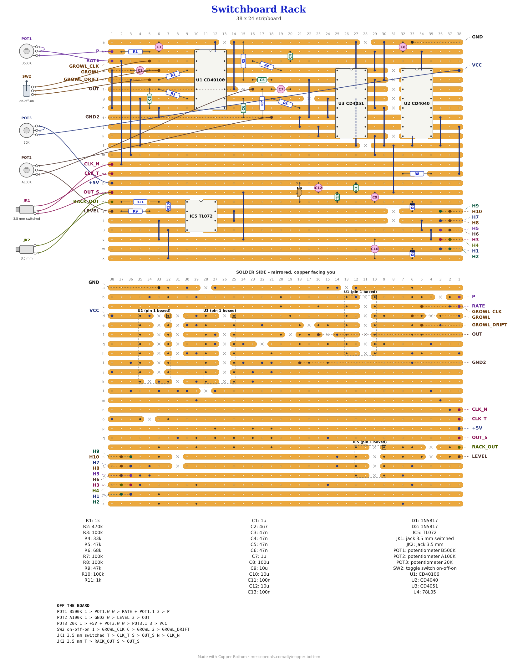
The Switchboard is four fixed 40106 oscillators and a 4051 that picks one at a time, walked by a 4040 counter on a fifth gate's clock: tone, rest, tone, rest, with a slow sixth gate swapping which pair of voices plays. On the bench it sounds beepy and clicky, and the growl toggle turns that into a robot and a fuzzy growl. In a rack the same board takes a clock from anything that ticks, and comes out at rack level.
What you'll need
tap to expand / collapse
On the board, counted from the layout file:
- 1× CD40106 hex Schmitt inverter, 14-pin DIP (U1)
- 1× CD4051 eight-way analog switch, 16-pin DIP (U3)
- 1× CD4040 twelve-stage binary counter, 16-pin DIP (U2)
- 1× TL072 dual op-amp, 8-pin DIP - spot it: TL072 printed on top, notch marks pin 1. An NE5532 or TL082 sits in the same holes (IC5)
- 4× 100k (brown-black-yellow; R3, R7 to R8, R10)
- 2× 1k (brown-black-red; R1, R11)
- 1× 33k (orange-orange-orange; R4)
- 1× 470k (yellow-violet-yellow; R2)
- 2× 47k (yellow-violet-orange; R5, R9)
- 1× 68k (blue-gray-orange; R6)
- 2× 100n ceramic disc (104; C11, C13)
- 4× 47n ceramic MLCC (473; C3 to C6)
- 1× 100u electrolytic (C8) - spot it: the stripe marks the negative leg
- 3× 10u electrolytic (C9 to C10, C12) - spot it: the stripe marks the negative leg
- 2× 1u electrolytic (C1, C7) - spot it: the stripe marks the negative leg
- 1× 4u7 electrolytic (C2) - spot it: the stripe marks the negative leg
- 2× 1N5817 Schottky, the reverse-polarity diode - spot it: a fat black body, band toward the cathode (D1 to D2)
- 1× 78L05 5 V regulator, TO-92 - spot it: 78L05 on the flat face; legs OUT, GND, IN. On this board they stand in one column across three strips, so left-to-right will not help you: OUT is the TOP leg, on the regulated rail, and IN is the BOTTOM leg, on the raw rail from the header. Backwards it gets very hot and the chip never sees 5 V, so check it before you power up (U4)
- 29 wire links (J1 to J21, J23 to J30) - solid core, tinned
- 1× 2×5 pin header, plain, 0.1″ - the Eurorack power connector. spot it: ten square pins in two rows. Not the shrouded kind; a shroud is 20 mm long and would cover the neighboring strips
- Stripboard, 24 strips × 38 holes or larger
Off the board
- 1× B500K 9 mm Alpha pot, the step rate, wired as a variable resistor: lug 3 and the wiper, the wiper jumpered to lug 1. R1 is its 1K floor
- 1× A100K 9 mm Alpha pot, the level, all three lugs used
- 1× 20K 9 mm Alpha pot, the starve, wired as a variable resistor: lug 1 and the wiper jumpered together to +5V, lug 3 to VCC
- 1× on-off-on sub-mini toggle, the growl: center lug to GROWL, the outer lugs to GROWL_CLK and GROWL_DRIFT
- 2× Thonkiconn PJ398SM 3.5 mm jacks: clock in, which uses the switch contact, and out
- 1× 8 HP Eurorack blank panel, three knobs, and a Eurorack power cable
What is the Switchboard, and what is new
Strips 0 to 13 are Switchboard.json hole for hole, growl pads and all; every net of the
Switchboard is re-derived from the new copper before this page is written. Off came D1 and the
+9V pad, the old reverse-polarity diode, because the header brings its own two, and one link, J22,
which carried the clock down to the 4040. The rack block sits on ten new strips under the board
rather than beside it, because the board is already 38 holes long and a module's board has to
fit behind the panel between the rails.
Clock in. J22 is now a normalled jack, the Spider Rack's way. The 40106's clock leaves on the CLK_N pad to the jack's switch contact, and the jack's tip comes back on CLK_T through 100K (R8) to the 4040. With nothing plugged in, the jack's own switch joins the two and the rate knob runs the steps as before; plug in a rack clock or gate and it takes over, the 100K limiting what the chip's input diodes see. The growl toggle still works on the board's own clock line, whichever clock is counting.
The starve. The 78L05's output does not go straight to the chips: it leaves on the +5V pad to the starve pot, and comes back on VCC. So the module needs that pot, or a wire from +5V to VCC in its place, to make any sound at all. I chose 20K for it at 9 V; at 5 V the chips will give out sooner in the turn, and the bench will say whether 20K is still right.
Level. C7 and R7 stay, so the level pot is wired exactly as on the box, but its wiper now goes through 47K into the TL072 with 100K feedback, a gain of about two. The mux puts out a 0 to 5 V square, which after C7 is about ±2.5 V, so the top of the knob is about ±5 V.
The layout file is the guide
As on every stripboard guide here, the build document is the file itself: ↓ Download Switchboard_Rack.json - import it into Copper Bottom and the editor gives you the board picture, the placement walkthrough, the electrical checks and a printable build sheet, all from the same file. No coordinates are written out on this page on purpose: the editor is the viewer, and a number typed twice is a number that can drift.
The netlist
Quoted verbatim from the layout file. It was written from the board, so checking the board against it can only pass - what it is for is carrying the circuit somewhere else, and telling you what each strip is supposed to be doing while you stare at it. The bug board's nets keep the names they have on its own page.
The off-board wiring
25 pads leave the board. Ten of them are the power header, and two are test points or carry nothing off the board.
| Pad | Goes to |
|---|---|
| P, RATE | The rate pot, as on the Switchboard: lug 3 to P, wiper to RATE, wiper jumpered to lug 1 |
| OUT, GND2, LEVEL | The level pot: lug 3 to OUT, lug 1 to GND2, and the wiper to LEVEL, into the op-amp through R9 |
| GROWL, GROWL_CLK, GROWL_DRIFT | The growl toggle, an on-off-on: center lug to GROWL, on the drift oscillator's timing node; the outer lugs to GROWL_CLK, the clock line, and GROWL_DRIFT, the drift output. Center off is the board without it |
| +5V, VCC | The starve pot: lug 1 and the wiper to +5V, the 78L05's output; lug 3 to VCC, the chips' supply. No pot, no sound: a wire across the two pads runs the module unstarved |
| CLK_T, CLK_N | The clock jack, a switched one: tip to CLK_T, switch contact to CLK_N. Nothing plugged, the switch joins them and the board clocks itself |
| H1 … H10 | The power header, 2×5, pins down the strips. H1 and H2 are -12 V and take the cable's red stripe, on the bottom strip; H3 to H8 are ground; H9 and H10 are +12 V |
| RACK_OUT | The output jack, tip. The four voices, about ±5 V, through the 1K |
| OUT_S | The two jacks' sleeves: ground |
| GND | Ground on the Switchboard's own strip; a test point, nothing leaves the board here |
The panel
8 HP, which is 40.6 mm of a 128.5 mm blank - Amplified Parts sells reversible black-and-aluminum blanks in every width from 2 to 20 HP. The template is drawn for 9 mm Alpha pots (7 mm holes), Thonkiconn jacks (6 mm), sub-mini toggles (6.5 mm) and 5 mm LEDs, with the rack's rails kept clear top and bottom and the four M3 mounting holes where Doepfer puts them. I/O along the bottom, controls above, as everything on this site does it.
↓ switchboard-rack-panel.pdf
Nobody has drilled this one yet - the holes are the module's pads, where they sit is the format applied to them.
The rack block, the same on every module
The bottom ten strips of this board are the rack block every module on this shelf carries, drawn here under the board instead of beside it. The 2×5 header takes the rack's power cable, mounted with its pins running down the strips so each pair of pins lands on one strip: -12 V, then three grounds, then +12 V. That is the only way it can go on stripboard - turned the other way, the -12 and ground pins would share copper. The red stripe on the cable goes to H1 and H2. A 1N5817 stands in series with each rail so a cable put on backwards does nothing instead of everything. A 78L05 then makes a 5 V rail for the chip, and a TL072 on the real ±12 V does the rack-level work.
Five volts for the CMOS, not twelve, is what makes these rack-polite for free. A CD4000-series input switches near half its supply, so a +5 V gate from a sequencer clocks a 5 V chip directly but would never reach the ~7 V a 12 V chip wants; a pot across 5 V makes exactly the 0 to 5 V control voltage every rack sequencer speaks; and a hot or negative rack signal into a CMOS input needs only a 100K in series, the chip's own input diodes doing the clamping at well under a tenth of a milliamp. It is also a change from the 9 V these boards were built at - every chip is rated down to 3 V so the circuits are fine, but the oscillators will sit at slightly different pitches, and that is one of the things the bench is for.
The IDC socket on the power cable overhangs the header by about two strips at each end. Nothing tall stands there - the generator that drew this refuses to put anything standing under the socket - so keep it that way if you move a part.
Check the cuts under the chips before the first power-up, with a meter. A DIP on stripboard puts pin 1 and the last pin on one strip, pin 2 and the one before it on the next, and so on down - each pair held apart by nothing but the chip's own cut. On an op-amp that puts pin 4 and pin 5 on the same strip, which here means the negative rail a whisker of copper away from ground. It is the normal shape of every stripboard op-amp build and it is fine when the cut is clean, but a cut that did not quite go through is a dead short across the supply with no resistor anywhere to survive it. Cut them, then measure each one - a track cutter leaves a hair at the edge of the hole more often than it looks.
How it works, in one breath
Four gates of the 40106 are four oscillators on fixed resistors and 47n caps, four pitches. A fifth gate is the clock, on the rate pot. The 4040 counts it, and two of its outputs drive two of the 4051's address pins, so the mux steps through four of its inputs: two are voices and two are ground, which is the tone-rest pattern. The sixth gate is a slow drift on the third address pin, swapping which two voices take the tone steps. The growl toggle joins the drift oscillator's timing node to the clock line, or straight to its own output, and that is where the robot and the growl come from. In the rack all of that runs at 5 V through the starve pot, and the TL072 doubles the mux's output to rack level.
Things to try
- Clock it from the Spider. The Spider Rack's CLK OUT into CLK IN and the two step together; its CV OUT does nothing here
- Audio-rate clock. Patch an oscillator into CLK IN and the steps blur into a tone of their own
- A deeper starve. A bigger pot in place of the 20K reaches further toward the point where the chips give out. Untested; the 20K is the one I have heard, at 9 V
The Switchboard is the layout of that name from this site: a 40106, a 4040 and a 4051 in the Lunetta way, with the growl and the starve from my bench build. The rack block is the standard DIY Eurorack power entry and an inverting op-amp stage. Drawn in Copper Bottom.