Quacker
An envelope filter on two 4558s · By Onion Madder · Mess O' Pedals
An envelope filter is a wah your playing works instead of your foot: dig in and the filter jumps open, ease off and it falls shut. This one is PedalPCB's Duck Box circuit, their take on the Guyatone WR3, with every part and value as they list it, moved onto a 17 by 25 stripboard. Two knobs, Attack and Decay, and a Blend toggle that mixes the dry signal back in.
It is the best envelope filter I have built, and it sounds amazing with both guitar and my synths. My own stripboard Envelope Filter does not come close, so this is that circuit for anyone who wants it without the PCB. Every part has the same name here as on PedalPCB's board, so their build document and this page can be read side by side.
What you'll need
tap to expand / collapse
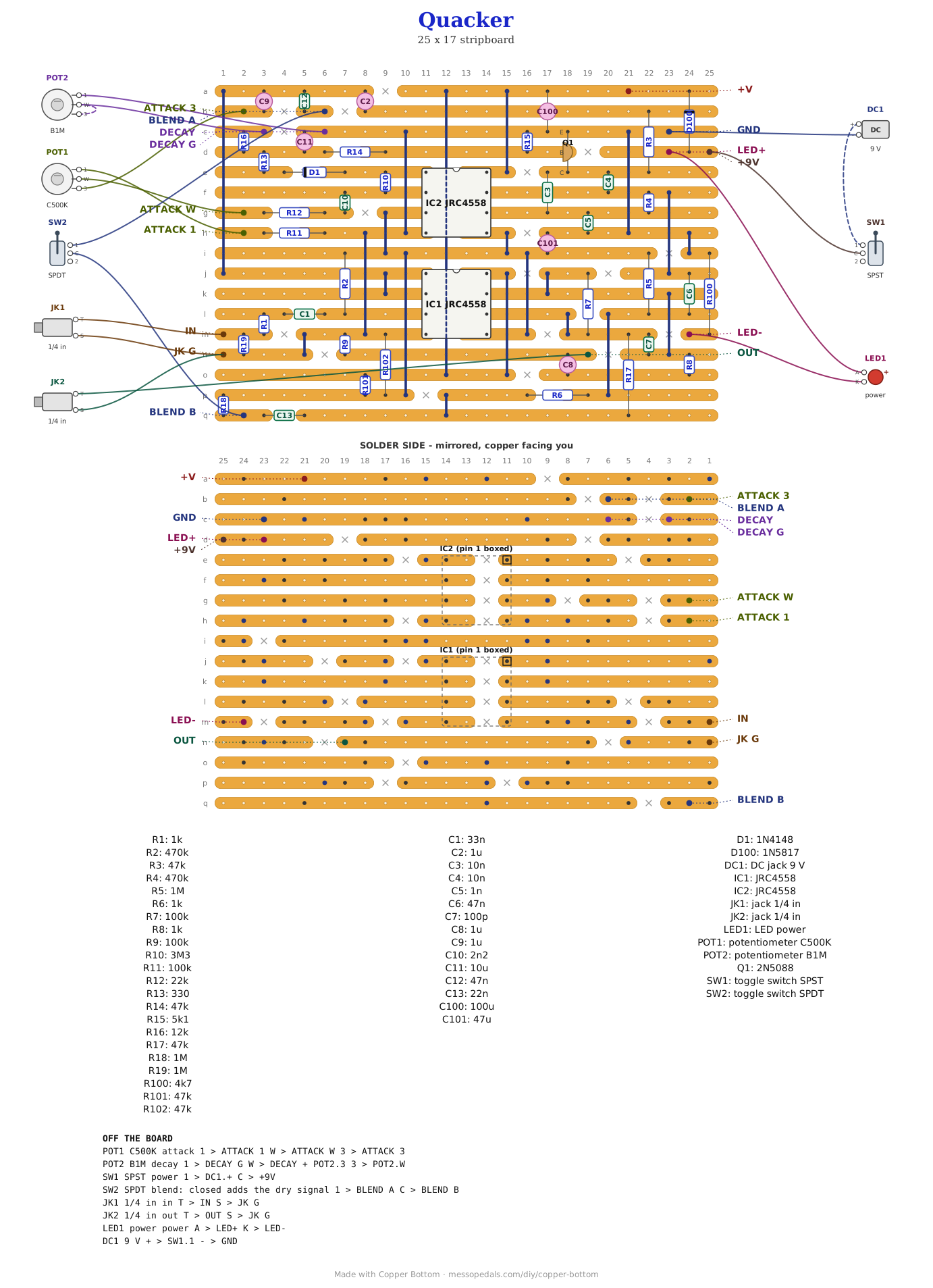
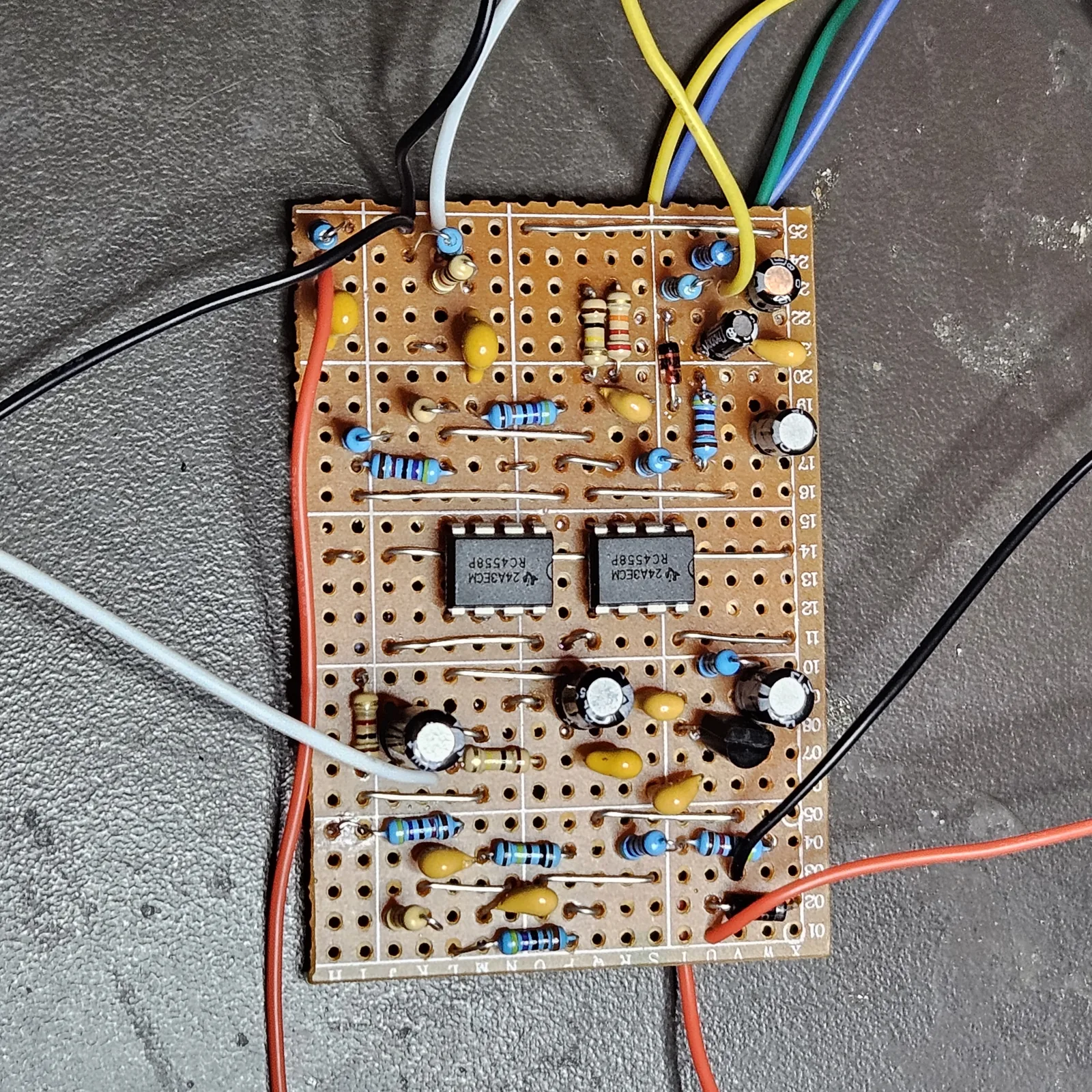
Forty-two parts on the board plus 20 wire links, and eight off it. The values are PedalPCB's, all of them; leave them as they are.
- 2× 4558 dual op-amp, DIP-8 (IC1, IC2) - spot it: eight legs, 4558 in the number on top (JRC4558, NJM4558, RC4558), a notch or a dot at the pin 1 end. IC1 is the input buffer and the output stage; IC2 is the filter and the envelope amplifier. They solder straight to the board
- 1× 2N5088 NPN transistor (Q1) - spot it: a black half-round TO-92, 2N5088 on the flat face. Flat face toward you, the legs are E, B, C left to right. It is the knob the envelope turns: the more it conducts, the higher the filter sits
- 1× 1N4148 (D1) - spot it: a tiny orange glass body with a black band. It rectifies the envelope. PedalPCB lists a DS448 and names the 1N4148 as the alternate
- 1× 1N5817 Schottky (D100) - spot it: fat black body, a gray band at one end. Reverse-polarity protection on the supply
- 3× 1M resistor (R5, R18, R19) - spot it: bands brown-black-green. R19 holds the input jack at ground; R5 and R18 hold the output stage's two coupling caps at the reference
- 2× 470K resistor (R2, R4) - spot it: bands yellow-violet-yellow. R2 biases the input buffer; R4 is the filter's feedback, and it sets how narrow the filter is
- 1× 3M3 resistor (R10) - spot it: bands orange-orange-green. The envelope amplifier's feedback: with R12 it gives a gain of 150
- 3× 100K resistor (R7, R9, R11) - spot it: bands brown-black-yellow. R7 is the output stage's feedback, R9 holds the output jack at ground, and R11 sits under the Attack pot
- 5× 47K resistor (R3, R14, R17, R101, R102) - spot it: bands yellow-violet-orange. R101 and R102 make the half-supply reference; R3 feeds the filter; R14 carries the envelope to Q1; R17 feeds the output stage
- 1× 22K resistor (R12) - spot it: bands red-red-orange. Into the envelope amplifier
- 1× 12K resistor (R16) - spot it: bands brown-red-orange. The floor under the Decay pot, so the shortest decay is not a short
- 1× 5K1 resistor (R15) - spot it: bands green-brown-red. With R14 it divides the envelope down for Q1's base
- 1× 4K7 resistor (R100) - spot it: bands yellow-violet-red. The power LED's resistor, on the LED's short-leg side
- 3× 1K resistor (R1, R6, R8) - spot it: bands brown-black-red
- 1× 330Ω resistor (R13) - spot it: bands orange-orange-brown. It lets the envelope cap fill fast, which is the snap on every note
- 2× 47nF film (C6, C12) - spot it: a box printed 473
- 1× 33nF film (C1) - spot it: printed 333
- 1× 22nF film (C13) - spot it: printed 223
- 2× 10nF film (C3, C4) - spot it: printed 103. The filter's two caps: change them only as a pair
- 1× 2.2nF film (C10) - spot it: printed 222. It makes the envelope listen to the bright edge of each note
- 1× 1nF film (C5) - spot it: printed 102
- 1× 100pF ceramic (C7) - spot it: a small disc printed 101
- 3× 1 µF electrolytic (C2, C8, C9) - spot it: a small can with a stripe down one side; the stripe leg is the negative one. C2 and C9 take the buffered signal to the filter and the Attack pot; C8 is the output cap
- 1× 10 µF electrolytic (C11) - spot it: the same kind of can. The envelope cap: D1 fills it, the Decay pot drains it. Stripe to ground
- 1× 47 µF electrolytic (C101) - spot it: a bigger can. Holds the reference quiet. Stripe to ground
- 1× 100 µF electrolytic (C100) - spot it: the biggest can. The supply reservoir. Stripe to ground
- 20× wire links - offcuts of component leg. One of them, J12, runs under both chips, so it goes in before either chip does
Off the board
- 1× C500K reverse-log pot - Attack. A C on the back means reverse log, which is what PedalPCB lists. Lug 3 to ATTACK 3, wiper to ATTACK W, lug 1 to ATTACK 1. It sets how much of your signal reaches the envelope, so it is how hard you have to play to open the filter
- 1× B1M linear pot - Decay. A variable resistor: wiper and lug 3 joined, both to DECAY; lug 1 to DECAY G. R16 on the board is its floor
- 1× SPDT on-on toggle - Blend, as on PedalPCB's board, which uses two of its lugs; an SPST does the same job. Center lug to BLEND B, one side lug to BLEND A. Closed mixes the dry signal back in
- 2× 1/4 inch jacks - in on the left, out on the right. Input tip to IN, output tip to OUT, both sleeves to JK G
- 1× LED for power - long leg to LED+, short leg to LED-. R100 on the board sets its current
- 1× DC jack, 9 V center negative
- An SPST toggle for power, in the positive supply lead between the DC jack and the board's +9V pad. Every build on this shelf gets one, and the drawing above shows it
The layout file is the guide
Like every layout on this shelf, the build document for this one is the file itself: ↓ Download Quacker.json - import it into Copper Bottom and the editor gives you the board picture, the placement walkthrough, the electrical checks and a printable build sheet, all from the same file. No coordinates are written out on this page on purpose: the editor is the viewer, and a number typed twice is a number that can drift.
J12 runs under both chips, down the column between their pin rows from strip a to strip o, carrying the supply, so solder it before either chip goes in. The chips are stacked, IC2 above IC1. Strip a carries two things: on the left the buffered input, which J14 lifts from IC1's pin 1 up the left edge and which C9, C12 and C2 hang from, and on the right the supply after D100. The envelope crosses to Q1's base along strip d, above IC2. Q1 stands with its flat face the way Copper Bottom draws it, emitter on strip c, base on d, collector on e; check the picture before you solder it. The input comes in on the left and the output leaves on the right, the way the jacks go on my boxes.
The netlist
tap to expand / collapse
My script wrote this from PedalPCB's schematic and the board was checked against it in Copper Bottom: every connection it names is on the board and nothing on the board is missing from it. BUF is the buffered input, which goes three ways: to the filter, to the envelope and to the Blend toggle. FN is the filter's tuning node, where Q1 sits. ENV is the envelope on C11, and BASE is that envelope divided down for Q1. VREF is half the supply, which every op-amp input sits on.
The off-board wiring
Fifteen pads: the supply, a test point, the LED, the jacks, the two pots and the Blend toggle.
| Pad | Goes to |
|---|---|
| IN | The input jack tip. A guitar, a synth, another pedal |
| OUT | The output jack tip. There is no volume knob: the output stage brings the level back up |
| JK G | Both jack sleeves. Same net as GND |
| ATTACK 3 / W / 1 | The C500K Attack pot: lug 3, the wiper, lug 1 |
| DECAY / DECAY G | The B1M Decay pot: wiper and lug 3 joined to DECAY, lug 1 to DECAY G |
| BLEND A / BLEND B | The Blend toggle's two lugs. Closed is filter plus dry; open is the filter alone |
| LED+ / LED- | The power LED: long leg to LED+, short leg to LED- |
| +9V / GND | The supply, through the power toggle. DC jack positive to the toggle and the toggle to +9V; negative to GND |
| +V | A test point on the supply after D100. Nothing goes here |
Before you play
Switch it on with nothing plugged in: the LED should light. Then meter to ground. These numbers are arithmetic from the schematic, not off a built board.
| Meter | Expect |
|---|---|
| +V, and pin 8 of both chips | The supply less about 0.3 V, the drop across D100. About 8.7 V on 9 V |
| Pins 1, 2, 3, 5, 6 and 7 of both chips | About half of that, 4.3 V each. One near 0 or near the supply points at that op-amp's parts |
| C11's plus leg | About 3.6 V at rest. IC2 pin 1 sits at the reference and D1 passes it, so the envelope idles a diode below half supply |
| Q1's base, the middle leg | About 0.35 V at rest, just under where it turns on. Play hard and it should creep up toward 0.6 V |
How it works, in one breath
IC1's first half is a follower: the input comes in through R1 and C1, sits on the reference through R2, and leaves at pin 1 as BUF, a low-impedance copy that can feed three things at once. The filter is IC2's second half, wired as a bandpass with two 10nF caps: C3 into the inverting input, C4 back from the output, and R4 for feedback. The sound arrives through C2 and R3 at FN, the node between the two caps, and Q1 hangs from that node to ground. When Q1 is off, the filter sits low, around 100 Hz. As Q1 conducts it shunts that node harder, and the filter climbs past 1 kHz. In this kind of filter the width of the peak is set by R4 and the caps alone, so it stays the same narrow band as it climbs, and the higher it goes, the sharper it sounds. That is the vowel in the quack.
The envelope is IC2's first half. The Attack pot takes some of BUF through C9, and R12 with C10 pass only the top end, above about 3 kHz, so the envelope reacts to the bright click at the start of a note more than to the note itself. R10 gives that a gain of 150. D1 and R13 fill C11 almost instantly on every peak, and R16 with the Decay pot drain it again, alongside R14 and R15, which drain it too: anywhere from about a tenth of a second to about half a second. R14 and R15 divide C11 down to Q1's base, and because the op-amp idles at the reference, C11 idles a little below where Q1 turns on, so the filter is waiting at the edge and moves on the first note. IC1's second half is the output: C6 and R6 bring the filter in, R17 into the inverting input, R7 and C7 for feedback, a gain of about two to make up the level, and C8 to the jack. With Blend closed, C12 and C13 put some of BUF in beside the filter.
Things to try
None of these have been tried on this board, or on PedalPCB's.
- Move the sweep. C3 and C4 together set where it sweeps: 22nF both puts it about an octave lower, 4.7nF an octave higher. Change both or neither
- A wider quack. R4 sets how narrow the peak is: 220K roughly doubles its width for a softer, less vocal sweep
- Into a synth's line level. A hot synth will open the filter all the way with Attack only a little up. Turn Attack down rather than the synth
The same circuit on a breadboard
tap to expand / collapse
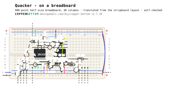
Want to hear it before you solder it? This is the layout file above moved onto a half-size breadboard, 30 columns by Copper Bottom's to breadboard button, in 69 steps with exact holes. It is a translation, not a copy: a strip and a breadboard column are different shapes, so every part is placed fresh and the stripboard's wire links are not needed.
Checked by the app, not built by me. Copper Bottom rebuilt the connections from these holes alone and compared them with the stripboard: all 112 terminals land on the same nets. Nobody has built this breadboard version.
Note. +9V is a second positive supply net. A breadboard rail carries one net, and the + rail here is +V, so +9V rides ordinary columns - follow its steps, not the rail.
Turn the board so the numbers climb left to right. Then A to E is the lower bank, F to J the upper, the top rails are above J and the bottom rails below A.
The semiconductors
| Step | Do |
|---|---|
| 1 | Seat IC1 (JRC4558) across the center channel, notch to the LEFT: pin 1 in E8, pin 8 in F8. Pins 1-4 run E8 to E11; pins 5-8 run back F11 to F8. Anywhere in the same bank and column is the same point - E8 and A8 are both pin 1. |
| 2 | Seat IC2 (JRC4558) across the center channel, notch to the LEFT: pin 1 in E15, pin 8 in F15. Pins 1-4 run E15 to E18; pins 5-8 run back F18 to F15. Anywhere in the same bank and column is the same point - E15 and A15 are both pin 1. |
| 3 | Diode D1 (1N4148): C15 to C19. The SECOND hole named gets the banded end - the cathode. Backwards, nothing works at all. |
| 4 | Diode D100 (1N5817): C2 to bottom + rail. |
| 5 | Transistor Q1 (2N5088): flat face toward you, legs E/B/C left to right into C12, C13, C14. The leg order is the package order, read with the flat face toward you and legs down. Check any device you are unsure of against its datasheet. |
Jumpers
| Step | Do |
|---|---|
| 6 | Jumper: A8 to A9 (C2.A to IC1.2). |
| 7 | Jumper: J8 to the top + rail (IC1.8 to +V). |
| 8 | Jumper: J15 to the top + rail (IC2.8 to +V). |
| 9 | Jumper: A11 to the bottom − rail (IC1.4 to GND). |
| 10 | Jumper: A12 to the bottom − rail (Q1.E to GND). |
| 11 | Jumper: A18 to the bottom − rail (IC2.4 to GND). |
| 12 | Jumper: J18 to A17 (IC2.5 to R102.A). |
| 13 | Jumper: I18 to J11 (IC2.5 to IC1.5). |
| 14 | Jumper: tie the top + rail to the bottom + rail at the right-hand end, so they are one rail. |
| 15 | Jumper: tie the top − rail to the bottom − rail at the right-hand end, so they are one rail. |
Resistors
| Step | Do |
|---|---|
| 16 | Resistor R1 (1k): C3 to C6. |
| 17 | Resistor R2 (470k): C10 to C17. |
| 18 | Resistor R3 (47k): B20 to B14. |
| 19 | Resistor R4 (470k): H16 to H17. |
| 20 | Resistor R5 (1M): H14 to H11. |
| 21 | Resistor R6 (1k): I14 to I19. |
| 22 | Resistor R7 (100k): H9 to H10. |
| 23 | Resistor R8 (1k): I9 to I6. |
| 24 | Resistor R9 (100k): C4 to bottom − rail. |
| 25 | Resistor R10 (3M3): B15 to B16. |
| 26 | Resistor R11 (100k): C5 to bottom − rail. |
| 27 | Resistor R12 (22k): C7 to C21. |
| 28 | Resistor R13 (330): B19 to B22. |
| 29 | Resistor R14 (47k): C22 to B13. |
| 30 | Resistor R15 (5k1): D13 to bottom − rail. |
| 31 | Resistor R16 (12k): D22 to D25. |
| 32 | Resistor R17 (47k): H19 to I10. |
| 33 | Resistor R18 (1M): I7 to I11. |
| 34 | Resistor R19 (1M): B3 to bottom − rail. |
| 35 | Resistor R100 (4k7): C23 to bottom − rail. |
| 36 | Resistor R101 (47k): top + rail to G11. |
| 37 | Resistor R102 (47k): B17 to bottom − rail. |
Ceramics and film
| Step | Do |
|---|---|
| 38 | Cap C1 (33n): B6 to B10. |
| 39 | Cap C3 (10n): D14 to I17. |
| 40 | Cap C4 (10n): A14 to I16. |
| 41 | Cap C5 (1n): G17 to top − rail. |
| 42 | Cap C6 (47n): G16 to G14. |
| 43 | Cap C7 (100p ceramic disc): G9 to G10. |
| 44 | Cap C10 (2n2): B21 to C16. |
| 45 | Cap C12 (47n): C8 to C24. |
| 46 | Cap C13 (22n): G19 to G7. |
Electrolytics
| Step | Do |
|---|---|
| 47 | Cap C2 (1u): + leg into B8, − leg into C20. The stripe on the can marks the MINUS leg. Backwards, an electrolytic eventually vents. |
| 48 | Cap C8 (1u): + leg into H6, − leg into B4. |
| 49 | Cap C9 (1u): + leg into D8, − leg into D26. |
| 50 | Cap C11 (10u): + leg into A22, − leg into the bottom − rail. |
| 51 | Cap C100 (100u): + leg into the bottom + rail, − leg into the bottom − rail. |
| 52 | Cap C101 (47u): + leg into D17, − leg into the bottom − rail. |
Off-board
| Step | Do |
|---|---|
| 53 | Wire for +9V: into A2. This is where DC jack +, through the power switch joins the board. |
| 54 | Wire for ATTACK 1: into A5. This is where ATTACK pot lug 1 joins the board. |
| 55 | Wire for ATTACK 3: into A26. This is where ATTACK pot (C500K) lug 3 joins the board. |
| 56 | Wire for ATTACK W: into A7. This is where ATTACK pot wiper (lug 2) joins the board. |
| 57 | Wire for BLEND A: into A24. This is where BLEND toggle, one lug: closed mixes the dry signal back in joins the board. |
| 58 | Wire for BLEND B: into J7. This is where BLEND toggle, the other lug (the center lug of an on-on SPDT) joins the board. |
| 59 | Wire for DECAY: into A25. This is where DECAY pot (B1M) wiper and lug 3, joined joins the board. |
| 60 | Wire for IN: into A3. This is where input jack tip joins the board. |
| 61 | Wire for LED-: into A23. This is where power LED short leg (cathode); R100 on the board takes it to ground joins the board. |
| 62 | Wire for LED+: into B2. This is where power LED long leg (anode) joins the board. |
| 63 | Wire for OUT: into A4. This is where output jack tip joins the board. |
| 64 | Wire for DECAY G: into the bottom − rail. This is where DECAY pot lug 1 joins the board. |
| 65 | Wire for JK G: into the bottom − rail. This is where both jack sleeves joins the board. |
Power up
| Step | Do |
|---|---|
| 66 | +V - a test pad on the supply after D100; nothing else: clip to the bottom + rail. |
| 67 | GND - DC jack - (center pin, 9V center-negative pedal supply): clip to the bottom − rail. |
| 68 | Before the battery: meter on continuity. rail to rail reads open, not a short A8 to A9 beeps (C2.A to IC1.2) J8 to top + rail beeps (IC1.8 to +V) J15 to top + rail beeps (IC2.8 to +V) A11 to bottom − rail beeps (IC1.4 to GND) A12 to bottom − rail beeps (Q1.E to GND) A18 to bottom − rail beeps (IC2.4 to GND) J18 to A17 beeps (IC2.5 to R102.A) I18 to J11 beeps (IC2.5 to IC1.5) |
| 69 | Power on. |
Translated by Copper Bottom v1.7.29 from Quacker.json.
The circuit is PedalPCB's Duck Box Filter, their take on the Guyatone WR3 Wah Rocker, built here from their published schematic with their part numbers and values. PedalPCB is not involved with this page and does not endorse it; buy their board if you would rather build it on a PCB. The stripboard layout and the words are mine, and so is anything wrong with them.