Envelope Filter
Two chips, four knobs, a filter that opens when you dig in · By Onion Madder · Mess O' Pedals
The sound is the quack: a filter whose cutoff follows how hard you play, so every note starts bright and closes down as it fades. This is the state-variable filter every synth book draws, two integrators in a loop, with the two halves of an LM13700 doing the integrating, because an OTA's gain is set by a current and a current is easy to steer with an envelope. The TL072 buffers the guitar and then amplifies it into a rectifier, the rectifier charges a cap, and that cap's voltage becomes the bias current for both OTAs. Four knobs: sensitivity sets how much signal it takes to open the filter, Q is resonance, range is where the sweep starts, and level. A toggle picks the bandpass output, which is the quack, or the lowpass, which is more of a sweep.
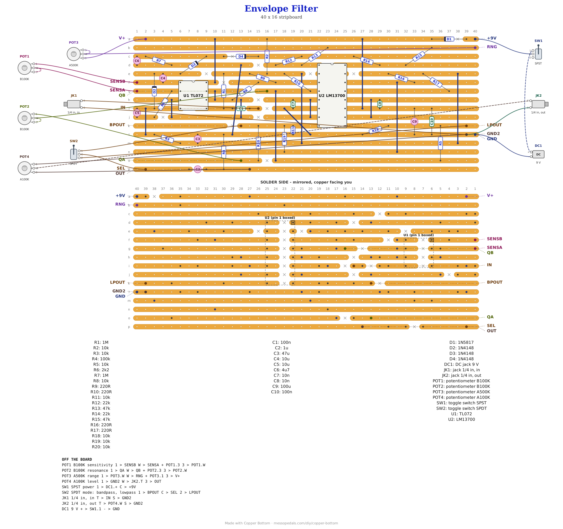
What you'll need
tap to expand / collapse
Thirty-four parts on the board plus the links, and nine off it. The OTA is the one to buy carefully, and the four 220Ω resistors are not optional.
- 1× LM13700 dual OTA, DIP-16 (U2) - spot it: sixteen legs, the number printed on top, a notch at one end. Its rails are pins 6 and 11, not the corners, and the layout file knows that. An LM13600 is the same pinout with a slightly different buffer and will work. Fit a socket
- 1× TL072 dual op-amp, DIP-8 (U1) - spot it: eight legs, notch at one end. One half buffers the input, the other is the sensitivity amplifier. Any dual op-amp with this pinout will do here; a TL072 is fine because nothing on this board asks it to reach a rail. Fit a socket
- 1× 1N5817 Schottky (D1) - spot it: fat black body, a gray band at one end. Reverse-polarity protection on the supply
- 3× 1N4148 (D2, D3, D4) - spot it: a tiny orange glass body with a black band. D2 and D3 are the rectifier that turns the amplified signal into an envelope; D4 sits between the envelope and the OTAs so a little hum on the cap does not open the filter
- 2× 1M resistor (R1, R7) - spot it: bands brown-black-green. R1 biases the input to the half-supply reference; R7 is what bleeds the envelope cap down, so it sets the release
- 1× 100K resistor (R4) - spot it: bands brown-black-yellow. Ties the output to ground so the level pot has something to sit on
- 2× 47K resistor (R13, R15) - spot it: bands yellow-violet-orange. R13 and R15 carry the range pot's current into the two bias pins, one each
- 2× 22K resistor (R12, R14) - spot it: bands red-red-orange. R12 and R14 carry the envelope into the two bias pins, one each. Lower both for a wider sweep
- 8× 10K resistor (R2, R3, R5, R8, R11, R18, R19, R20) - spot it: bands brown-black-orange. The workhorses. R2 and R3 make the half-supply reference; R8 and R19 feed signal into each OTA; R5 is the lowpass feedback that closes the loop; R11 and R18 load the two buffers; R20 is the floor under the Q pot
- 1× 2K2 resistor (R6) - spot it: bands red-red-red. The floor under the sensitivity pot: with the pot at zero the amplifier's gain is one
- 4× 220Ω resistor (R9, R10, R16, R17) - spot it: bands red-red-brown. Four of them, R9, R10, R16, R17, one per OTA input, to the reference. With the 10K feeds they divide the signal down about 46 times, which is what keeps an OTA clean. Leave one out and that input clips
- 2× 10nF ceramic (C7, C8) - spot it: printed 103. C7 and C8 are the two integrator caps, one per OTA. Same value, or the filter is not a filter. Change both to move the range
- 2× 100nF ceramic (C1, C10) - spot it: printed 104. C1 couples the input; C10 decouples the chips
- 1× 1 µF electrolytic (C2) - spot it: a small can with a stripe down one side; the stripe leg is the negative one. The output coupling cap. Stripe toward the level pot
- 1× 4.7 µF electrolytic (C6) - spot it: a small can with a stripe down one side; the stripe leg is the negative one. C6 is the envelope cap. The rectifier fills it and R7 drains it. Bigger is slower both ways. Stripe to ground
- 2× 10 µF electrolytic (C4, C5) - spot it: a small can with a stripe down one side; the stripe leg is the negative one. C4 couples the sensitivity amplifier into the rectifier; C5 is the amplifier's ground return, so its gain at DC is one. Stripes: C4 toward the diodes, C5 to ground
- 1× 47 µF electrolytic (C3) - spot it: a small can with a stripe down one side; the stripe leg is the negative one. Holds the half-supply reference quiet. Stripe to ground
- 1× 100 µF electrolytic (C9) - spot it: a small can with a stripe down one side; the stripe leg is the negative one. The supply reservoir. Stripe to ground
- 14× wire links - offcuts of component leg
- 1× DIP-16 socket and 1× DIP-8 socket
Off the board
- 1× B100K linear pot - sensitivity. A variable resistor: lug 1 to SENSB, wiper to SENSA, and a short wire from the wiper to lug 3. It is the feedback resistor of the sensitivity amplifier
- 1× B100K linear pot - Q, the resonance. A variable resistor: lug 1 to QA, wiper to QB, wiper jumpered to lug 3. It sets how much bandpass is fed back
- 1× A500K log pot - range, where the sweep starts. A variable resistor from the supply: lug 3 to V+, wiper to RNG, wiper jumpered to lug 1
- 1× A100K log pot - level. Lug 3 to OUT, lug 1 to GND2, wiper to the output jack tip
- 1× SPDT toggle - mode. Center to SEL, one side to BPOUT for bandpass, the other to LPOUT for lowpass
- 2× 1/4 inch jacks - in and out. Tips to IN and the level wiper, sleeves to GND2
- 1× DC jack, 9 V center negative
- An SPST toggle for power, in the positive supply lead between the DC jack and the board's +9V pad. Every build on this shelf gets one, and the drawing above shows it
The layout file is the guide
Like every layout on this shelf, the build document for this one is the file itself: ↓ Download Envelope_Filter.json - import it into Copper Bottom and the editor gives you the board picture, the placement walkthrough, the electrical checks and a printable build sheet, all from the same file. No coordinates are written out on this page on purpose: the editor is the viewer, and a number typed twice is a number that can drift.
Ground is strip l. The GND and GND2 pads sit on it at the right-hand end, and the rest of the board reaches it through links. The V+ pad is a supply pad with a job - it is the range pot's top lug, and it also tells the checker that strip is a rail. Pins 2 and 15 of the LM13700 are left open: they are the linearizing diode bias pins, the datasheet says they may be, and the checker knows that as of v1.7.3.
The netlist
My script wrote this from the design and the board was checked against it in Copper Bottom: every connection it names is on the board and nothing on the board is missing from it. The lines that explain the circuit are ENV, the envelope cap and its bleed resistor, ENV2, the same voltage past D4 and into the two bias resistors, O1 and O2, where each OTA's output meets its own buffer input and an integrator cap, and VREF, the half-supply point that eight resistors hang off.
The off-board wiring
Fourteen pads leave the board: four pots, a toggle, two jacks, the supply, and a test point that doubles as the range pot's top lug.
| Pad | Goes to |
|---|---|
| SENSB / SENSA | The sensitivity pot. Lug 1 to SENSB, wiper to SENSA, wiper jumpered to lug 3. Variable resistor, not a divider |
| QA / QB | The Q pot. Lug 1 to QA, wiper to QB, wiper jumpered to lug 3 |
| V+ / RNG | The range pot. Lug 3 to V+, wiper to RNG, wiper jumpered to lug 1. V+ is the protected supply after D1 |
| SEL / BPOUT / LPOUT | The mode toggle. Center to SEL; BPOUT is the bandpass, the quack; LPOUT is the lowpass, the sweep |
| IN | Input jack tip, through your bypass switch if you fit one. The sleeve goes to GND2 |
| OUT | Level pot lug 3. The wiper goes to the output jack tip, and lug 1 to GND2 |
| GND2 | Level pot lug 1 and both jack sleeves. Same net as GND |
| +9V / GND | The supply, through the power toggle. DC jack positive to the toggle and the toggle to +9V; negative to GND |
How it works, in one breath
Half the TL072 is a follower that buffers the input, and its output goes two ways. One way is into the filter: through R8 and R9 the signal is divided down about 46 times and lands on the first OTA's plus input. The OTA turns that into a current, the current charges C7, and the buffer on pins 7 and 8 reads C7 out: that is one integrator, and its output is the bandpass. The bandpass goes through R19 and R16 into the second OTA, which integrates it onto C8 and reads it out through the buffer on pins 10 and 9: the lowpass. The lowpass comes back through R5 to the first OTA's minus input to close the loop, and the Q pot brings some bandpass back to the same point; less of it and the filter rings harder. Where the two integrators turn over depends on the current into pins 1 and 16, and that current is the whole point.
The other way the buffered signal goes is into the other half of the TL072, wired as an amplifier whose gain is one plus the sensitivity pot over R6, so anywhere from one to about 46. Its output goes through C4 to D2 and D3, which rectify it into C6: the envelope. R7 bleeds C6 down over a few seconds, so the filter closes after a note. That voltage goes through D4, which takes about half a volt off the top so that noise on the cap does not open the filter, and then through R12 and R14 into the two bias pins. The range pot adds a fixed current through R13 and R15 on top, so the filter is never fully closed, and the envelope sweeps it up from wherever range put it. That is what the schematic does, and it is a read of the circuit, not of a build.
Things to try
None of these have been tried, because none of this has. They are the obvious knobs.
- Change C7 and C8 together. 22n moves the whole sweep down an octave, 4n7 up
- Change C6 for a faster or slower filter. 1 µF closes quickly, 10 µF hangs on
- Lower R12 and R14 to 10K for a wider sweep, if the envelope runs out before the filter opens far enough
- Take the CD4094 out of the Rungler and put its stepped voltage into ENV2 through 47K instead of the envelope, and the filter steps instead of following
The OTA state-variable filter is in the LM13700 datasheet and every synth book since; the envelope follower opening one is the idea behind every auto-wah, from the Mu-Tron III down. The board is mine, drawn by my own script, and so is anything wrong with it.