Ladybug Rack
Audio in, CV out · A TL074 on seventeen strips · By Onion Madder · Mess O' Pedals
Patch a drum module, a VCO or a guitar into it and the CV jack follows how loud it is: up on every hit, down as it fades. The second jack is the same thing upside down, high in silence and dropping as the sound gets louder, which is what you want for ducking. Three knobs - sensitivity, attack, release - and an LED. It is the Ladybug on the stripboard shelf, the same four op-amps on a TL074 and the rack's real ±12 V.
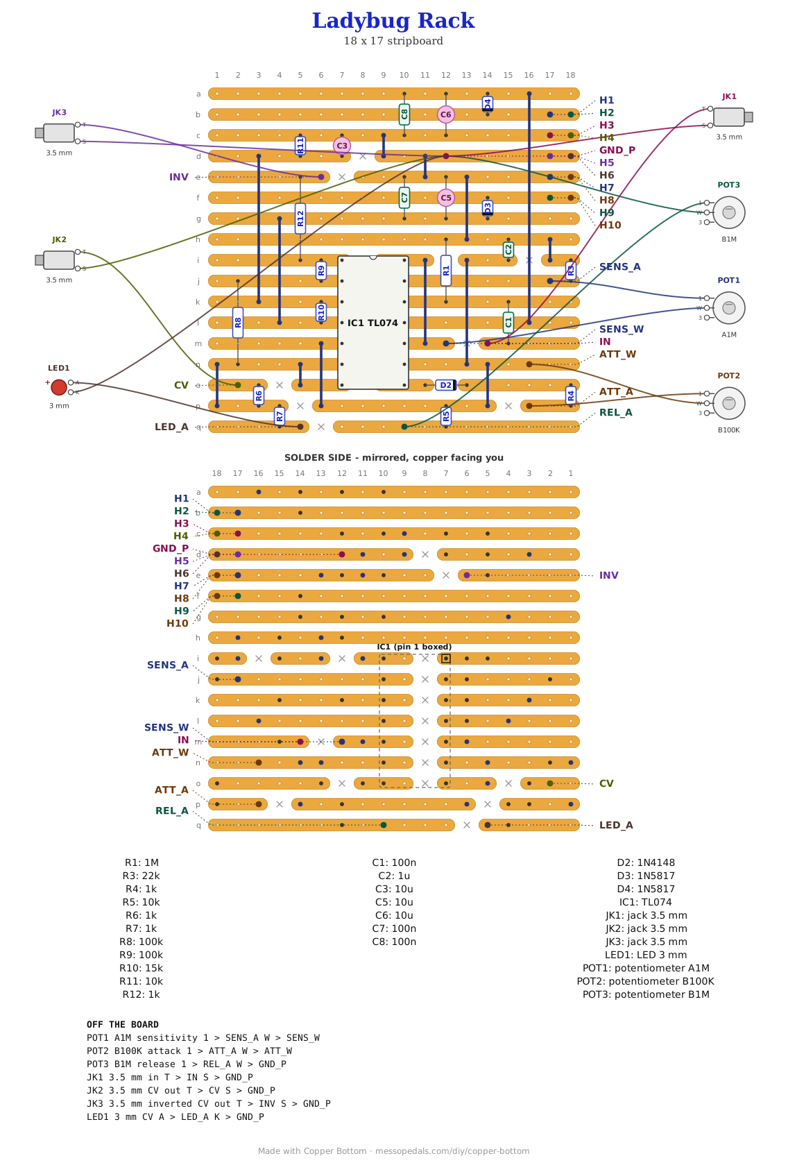
What you'll need
tap to expand / collapse
On the board, counted from the layout file:
- 1× TL074 quad op-amp, 14-pin DIP (IC1) - spot it: TL074 printed on top, a notch at pin 1. A TL084 sits in the same holes
- 2× 100k (brown-black-yellow; R8 to R9)
- 2× 10k (brown-black-orange; R5, R11)
- 1× 15k (brown-green-orange; R10)
- 1× 1M (brown-black-green; R1)
- 4× 1k (brown-black-red; R4, R6 to R7, R12)
- 1× 22k (red-red-orange; R3)
- 2× 100n ceramic disc (104; C7 to C8)
- 1× 100n box film (104; C1)
- 1× 1u box film (105, or a small film cap; C2)
- 3× 10u electrolytic (C3, C5 to C6) - spot it: the stripe marks the negative leg
- 1× 1N4148 signal diode - spot it: a tiny glass body, black band toward the cathode (D2)
- 2× 1N5817 Schottky, the reverse-polarity diode - spot it: a fat black body, band toward the cathode (D3 to D4)
- 13 wire links (J1 to J13) - solid core, tinned
- 1× 2×5 pin header, plain, 0.1″ - the Eurorack power connector. spot it: ten square pins in two rows. Not the shrouded kind; a shroud is 20 mm long and would cover the neighboring strips
- Stripboard, 17 strips × 18 holes or larger
Off the board
- 1× A1M 9 mm Alpha pot, SENSITIVITY, as a variable resistor: lug 1 to SENS_A, wiper to SENS_W, lug 3 empty
- 1× B100K 9 mm Alpha pot, ATTACK: lug 1 to ATT_A, wiper to ATT_W, lug 3 empty
- 1× B1M 9 mm Alpha pot, RELEASE: lug 1 to REL_A, wiper to GND_P, lug 3 empty
- 3× Thonkiconn PJ398SM 3.5 mm jacks: IN, CV OUT and INV OUT. Every sleeve to GND_P
- 1× 3 mm LED, long leg to LED_A, short leg to GND_P. Its 1K is on the board
- A Eurorack blank panel - three knobs, three jacks and an LED fit 8 HP - and a Eurorack power cable
What it is
Four op-amps, one job each. D (pins 12 to 14) is the sensitivity stage: the input sits at ground on R1 1M, C1 takes it in, and the SENSITIVITY pot over R3 22K gives a gain of 1 to about 46. C (pins 8 to 10) catches the peaks: it charges C2 through D2, R4 and the ATTACK pot, and reads C2 back on pin 9, so the diode sits inside the loop and its 0.6 V never comes off the CV. C2 drains through R5 and the RELEASE pot. B (pins 5 to 7) is a buffer, so the jack and the LED never pull on C2. A (pins 1 to 3) flips the CV around a reference of about 4.7 V from R10 and R11, so the inverted jack sits at about 9.4 V in silence and falls as the other one rises.
What changed from the 9 V box. On one supply that board's gain stage rectifies by flattening the negative halves at 0 V, and it needs a Schottky on its input to keep the chip from being dragged below ground. Here the input swings both ways inside the rails, so the clamp and its series resistor are gone; the peak catcher only ever charges C2 upward, so it is still a half-wave follower. Between peaks pin 8 swings down to about -10 V, and D2, a 1N4148, is good for far more than that the wrong way.
C2 is a film cap on purpose. An electrolytic leaks, and the leak would be a second release knob you cannot turn. Every time on this page - attack about 1 to 100 ms, release about 10 ms to a second - is the arithmetic of C2 and the pots, not a measurement.
The layout file is the guide
As on every stripboard guide here, the build document is the file itself: ↓ Download Ladybug_Rack.json - import it into Copper Bottom and the editor gives you the board picture, the placement walkthrough, the electrical checks and a printable build sheet, all from the same file. No coordinates are written out on this page on purpose: the editor is the viewer, and a number typed twice is a number that can drift.
The netlist
Quoted verbatim from the layout file. It was written from the design, so the editor's check that the
board matches it compares two separate records - what it is for is carrying the circuit somewhere else, and
telling you what each strip is supposed to be doing while you stare at it. HOLD is the capacitor
the CV lives on; PKO and PK are the two ends of the peak catcher's diode.
The off-board wiring
20 pads leave the board. Ten of them are the power header.
| Pad | Goes to |
|---|---|
| IN | Audio in, jack tip. Anything from a drum module to a VCO |
| SENS_A, SENS_W | The SENSITIVITY pot. Lug 1 and the wiper. Turned down is x1, up about x46 |
| ATT_A, ATT_W | The ATTACK pot. Lug 1 and the wiper. With the 1K on the board, about 1 to 100 ms |
| REL_A | The RELEASE pot. Lug 1 here, the wiper to GND_P. With the 10K on the board, about 10 ms to a second |
| CV | CV out, jack tip, through 1K. 0 to about 10 V, rising with the sound |
| INV | Inverted CV out, jack tip, through 1K. About 9.4 V in silence, falling as the sound rises |
| LED_A | The LED, long leg. It shows the CV |
| GND_P | Ground for the panel: the three jack sleeves, the LED's short leg and the RELEASE wiper |
| H1 … H10 | The power header, 2×5, pins down the strips. H1 and H2 are -12 V and take the cable's red stripe; H3 to H8 are ground; H9 and H10 are +12 V |
The rack block
The power sits along the top and the right of the board, the way it does on every module on this shelf. The 2×5 header takes the rack's power cable, mounted with its pins running down the strips so each pair of pins lands on one strip: -12 V, then three grounds, then +12 V. The red stripe on the cable goes to H1 and H2, on strip b at the top right. A 1N5817 stands in series with each rail so a cable put on backwards does nothing, and a 10 µF and a 100n sit on each rail. The three ground strips run the whole width of the board, which is where every ground on it lands. No regulator: a TL074 is happy on the rails as they come.
The IDC socket on the power cable overhangs the header by about two strips at each end. Nothing tall stands there, so keep it that way if you move a part.
Check the cuts under the chip before the first power-up, with a meter. On a TL074 pin 4 and pin 11 share a strip, +12 a whisker of copper from -12, held apart by nothing but the chip's own cut. A cut that did not quite go through is a dead short across the supply. Cut them, then measure each one.
How it works, in one breath
An envelope follower listens and reports. The gain stage decides how hard it listens, the peak catcher grabs the top of each wave and holds it on a capacitor, the release knob lets that hold leak away, and a buffer hands the result to the jack without disturbing it. Into a filter cutoff it is an auto-wah; into a VCA fed by something else it is a sidechain; inverted into that VCA, it is ducking.
Things to try
- Ducking. Kick drum into IN, INV OUT into a VCA carrying a pad, and the pad dips on every kick
- Auto-wah. A guitar or a VCO into IN, CV OUT into a filter's cutoff, and the filter opens as you play harder
- A longer release. C2 at 2.2 µF doubles every time on both knobs. Keep it film
- Into the box version's world. The Ladybug on stripboard does the same from 9 V, for the boxes on the shelf
The circuit is the textbook envelope follower - a gain stage, a peak detector with its diode inside the loop, a buffer - with an inverter added for the second out. The layout is Onion Madder's, drawn in Copper Bottom the same evening as the Ladybug it comes from.