Envelope Rack
Gate in, shape out · The built envelope on the bus · 8 HP · By Onion Madder · Mess O' Pedals
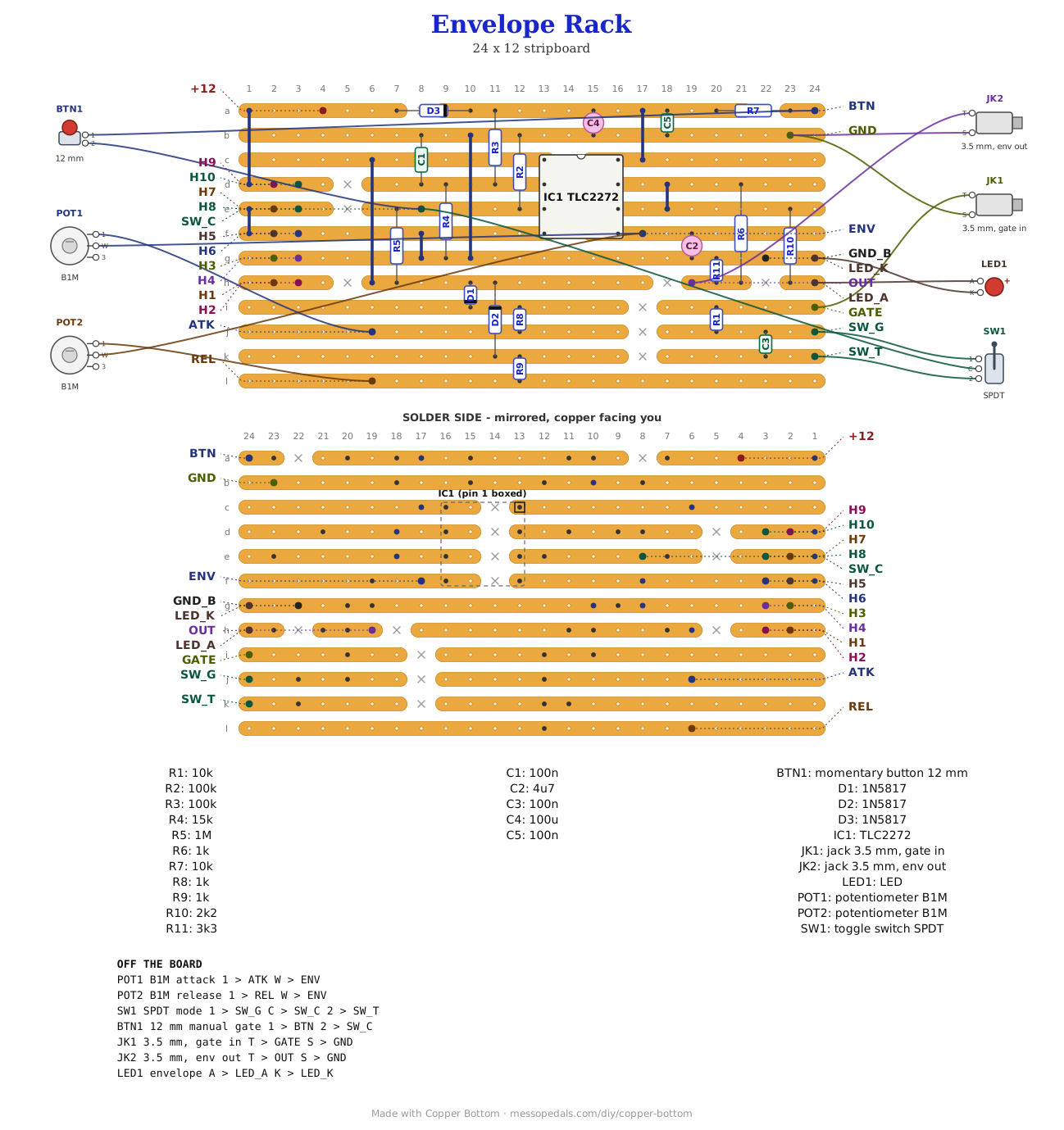
The AD/AR Envelope on the stripboard shelf runs from one 9 to 12 V supply on a rail-to-rail op-amp, and one 12 V supply is exactly what a rack has. So this is that board, the one I built, unchanged, with a power header on its left end and one resistor added to bring the output down to rack level. Two knobs, a toggle, a button, an LED and two jacks. Eight HP.
What you'll need
tap to expand / collapse
On the board, counted from the layout file:
- 1× TLC2272 rail-to-rail dual op-amp, 8-pin DIP - spot it: TLC2272 printed on top, notch marks pin 1. A TLC2262 or TLV2372 sits in the same holes; a TL072 will not work from one supply (IC1)
- 2× 100k (brown-black-yellow; R2 to R3)
- 2× 10k (brown-black-orange; R1, R7)
- 1× 15k (brown-green-orange; R4)
- 1× 1M (brown-black-green; R5)
- 3× 1k (brown-black-red; R6, R8 to R9)
- 1× 2k2 (red-red-red; R10)
- 1× 3k3 (orange-orange-red; R11)
- 3× 100n ceramic disc (104; C1, C3, C5)
- 1× 100u electrolytic (C4) - spot it: the stripe marks the negative leg
- 1× 4u7 electrolytic (C2) - spot it: the stripe marks the negative leg
- 3× 1N5817 Schottky: D1 and D2 steer the charge one way through each knob, D3 blocks a backwards cable - spot it: a fat black body, band toward the cathode (D1 to D3)
- 7 wire links (J1 to J7) - solid core, tinned
- 1× 2×5 pin header, plain, 0.1″ - the Eurorack power connector. spot it: ten square pins in two rows. Not the shrouded kind; a shroud is 20 mm long and would cover the neighboring strips
- Stripboard, 12 strips × 24 holes or larger
Off the board
- 2× B1M 9 mm Alpha pots, attack and release, each wired as a variable resistor: lug 1 to ATK or REL, both wipers to ENV, lug 3 empty. The 1K floor each one needs is on the board
- 1× sub-mini SPDT toggle, the mode switch: common to SW_C, one side to SW_G for AR, the other to SW_T for AD
- 1× 12 mm momentary push button, normally open, the manual gate: one lug to BTN, the other to SW_C
- 2× Thonkiconn PJ398SM 3.5 mm jacks, gate in and envelope out. Both sleeves to GND
- 1× 5 mm LED, long leg to LED_A, short leg to LED_K. Its 2K2 is on the board
- 1× 8 HP Eurorack blank panel, two knobs, and a Eurorack power cable
What it is
Columns 5 to 23 are AD_AR_Envelope.json hole for hole: same strips, same cuts,
same parts. The one thing that came off is the 9V pad, whose job the power
header does now. Link J6 carries +12 V from the header to the strip that
pad was on, ahead of D3, so the diode that stopped a backwards DC plug on the
stripboard build stops a backwards rack cable here. J7 ties the header's
spare ground pair into the envelope's ground.
R11 is the one new part inside the old board, a 3K3 standing in the one free hole on the output strip, down onto the ground strip beside it. It makes R6's 1K the top of a divider. The envelope peaks about a volt under the supply, near 10.5 V, and leaves the jack near 8 V with about 770 ohms behind it, which is where most rack envelopes sit.
The rack numbers, and they are arithmetic, not measurements. The gate has to clear the R3 and R4 divider, about 1.6 V on 12 V, so a 5 V or a 10 V rack gate fires it. A signal below ground goes through R1's 10K into the chip's own input diodes: -5 V makes half a milliamp, inside the 5 mA the datasheet allows. The 8 V top comes out a little lower with a TLC2262.
The layout file is the guide
As on every stripboard guide here, the build document is the file itself: ↓ Download Envelope_Rack.json - import it into Copper Bottom and the editor gives you the board picture, the placement walkthrough, the electrical checks and a printable build sheet, all from the same file. No coordinates are written out on this page on purpose: the editor is the viewer, and a number typed twice is a number that can drift.
The netlist
Quoted verbatim from the layout file. It was written from the board, so checking the
board against it can only pass - what it is for is carrying the circuit somewhere else, and
telling you what each strip is supposed to be doing while you stare at it. The envelope board's
nets keep the names they have on its own page;
+12_RAW is the bus supply ahead of D3, and -12_RAW goes nowhere.
The off-board wiring
24 pads leave the board. Ten of them are the power header.
| Pad | Goes to |
|---|---|
| ATK, REL, ENV | The two B1M pots. Attack: lug 1 to ATK, wiper to ENV. Release: lug 1 to REL, wiper to ENV. Two wipers on one pad, third lugs empty. Variable resistors, not dividers |
| SW_C, SW_G, SW_T | The mode toggle. Common to SW_C; SW_G is AR, the gate as it is; SW_T is AD, the gate through C3 so only its rising edge gets through |
| BTN | The manual button, one lug. The other lug goes to SW_C, so the button works in either mode |
| GATE | Gate in, jack tip. Any rack gate over about 1.6 V |
| OUT | Envelope out, jack tip. About 0 to 8 V, R6 over R11 |
| LED_A, LED_K | The LED, long leg to LED_A. It follows the envelope |
| GND, GND_B | Ground for the panel: both jack sleeves. GND_B is the same net, there if a wire is easier to land on that side |
| +12 | A test point on +12 V from the bus, before D3. Nothing leaves the board here |
| H1 … H10 | The power header, 2×5, pins down the strips. H1 and H2 are -12 V and take the cable's red stripe, on strip h, and nothing else uses them; H3 to H8 are ground; H9 and H10 are +12 V |
The panel
8 HP, which is 40.6 mm of a 128.5 mm blank - Amplified Parts sells reversible black-and-aluminum blanks in every width from 2 to 20 HP. The template is drawn for 9 mm Alpha pots (7 mm holes), Thonkiconn jacks (6 mm), sub-mini toggles (6.5 mm) and 5 mm LEDs, with the rack's rails kept clear top and bottom and the four M3 mounting holes where Doepfer puts them. I/O along the bottom, controls above, as everything on this site does it.
↓ envelope-rack-panel.pdf
Nobody has drilled this one yet - the holes are the module's pads, where they sit is the format applied to them.
The rack block
The left end of the board is the smallest rack block on this shelf. The 2×5 header takes the rack's power cable, mounted with its pins running down the strips so each pair of pins lands on one strip: -12 V, then three grounds, then +12 V. That is the only way it can go on stripboard - turned the other way, the -12 and ground pins would share copper. The red stripe on the cable goes to H1 and H2. There is no diode per rail, because D3 on the envelope board already stands in the +12 line, and -12 V is not used at all: a cable on backwards puts -12 on the +12 strip, where D3 blocks it, and +12 on a strip that goes nowhere. No regulator and no TL072 either - the envelope was drawn for one supply on a rail-to-rail chip, and +12 V is one supply.
The IDC socket on the power cable overhangs the header by about two strips at each end. Nothing tall stands there - the generator that drew this refuses to put anything standing under the socket - so keep it that way if you move a part.
Check the cuts under the chip before the first power-up, with a meter. On the TLC2272 the cut is all that keeps pin 1, the comparator's output, off pin 8's supply strip, and pin 5, the envelope, off pin 4's ground. A hair left in either one and the envelope will not move. Cut them, then measure each one.
How it works, in one breath
One half of the TLC2272 is a comparator watching the gate. When the gate goes high its output snaps to the supply and charges C2 through D1, R8 and the attack pot: that is the attack. When the gate goes low the output drops to ground and C2 drains the other way, through the release pot, R9 and D2: that is the release. The diodes keep the two knobs apart, one for each direction. The other half is a follower that copies C2 to the jack and the LED without taking anything from it. In AR the comparator sees the gate itself, so the envelope holds at the top for as long as the gate does; in AD the gate goes through C3 first, which passes a pulse of about 10 ms and nothing after it. That is a read of the circuit; what AD does on the bench is on the stripboard page when I have played with it more.
Things to try
- Change C2. It sets the whole range: 10 µF doubles every time, 1 µF makes it snappy and percussive
- Swap the pots for B500K. It halves the longest time and gives the short settings, where most of the playable ones live, more of the knob
- Clock it from the rack. A sequencer gate or the LFO Rack's square into GATE, and the out into a VCA or a filter, and every step gets its own swell
The circuit is Sam Battle's, the simple AD/AR from LookMumNoComputer, by way of Eddy Bergman's stripboard layout of it. The one-supply board, the rack block and the output divider are Onion Madder's, drawn in Copper Bottom.