Paper Beetle
A one-chip compressor as a heart-shaped paper circuit · By Onion Madder · Mess O' Pedals
A compressor on paper: soft notes come up, loud ones are held down, and a fading chord hangs on. One NE571 and its datasheet hook-up, a volume knob, and the jacks and power on wires.
What a paper circuit is
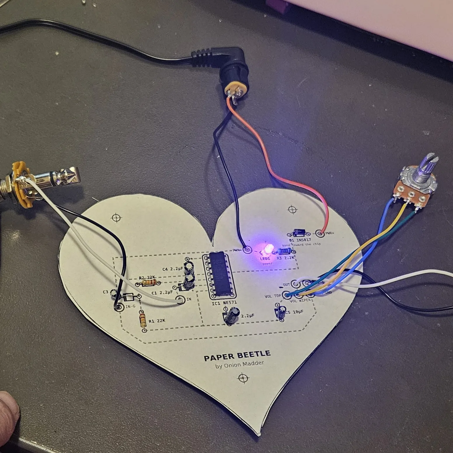
A paper circuit is a circuit board made of paper. The sheet you print is the board: the FRONT shows where every part sits, and the BACK is the same drawing mirrored, with the wiring on it. The printed front and back are glued to the two faces of a plain sheet folded in half, so the board is four sheets of paper thick, and every hole is poked through all four layers. The parts go in from the front, chips included, soldered straight to the paper. On the back, part legs bend along the printed lines, and bare wire covers the lines a leg cannot reach. Where one line has to cross another, an insulated wire hops over it. The power switch and the jacks hang off the board on wires. Nothing is etched and nothing is cut but paper: a printer, a glue stick, scissors, pointed tweezers, a cardboard box and a soldering iron are the whole kit.
The method is Peter Blasser's, from Ciat-Lonbarde. His paper circuits are a great idea, but they are complicated, full of unusual parts and hard to troubleshoot. This series takes circuits people already know, built from common parts, and makes a paper circuit something a beginner can try.
⚠ Before you start tap to expand / collapse
Paper burns. Keep the iron moving, quick joints, and don't rest it on the sheet. Work over something that isn't flammable, and keep a damp sponge handy.
Chip straight in. The NE571 is soldered straight to the paper with no socket, and a bare wire runs between its two rows of legs on the back. Keep each joint quick: touch, flow, lift.
Mind the cans. All five capacitors are polarized: the stripe is the − leg, and the sheet marks each + hole. C2's + leg goes to the output side, C4's to pin 1.
What you'll need
tap to expand / collapse
New to the parts? Each line notes how to spot it - the printed marking, the package, or the polarity clue.
- 1× NE571 compander (IC1) - spot it: NE571 printed on top, notch or dot at pin 1, 16 pins. An NE570 or SA571 has the same pins. It solders straight to the paper, no socket.
- Resistors: 2× 22K (R1, R2), 2.2K (R3) - spot it: 22K red-red-orange, 2.2K red-red-red. R1 and R2 set where the output sits; R3 feeds the power LED.
- 3× 2.2 µF electrolytic (C1, C2, C4) - spot it: little cans; the stripe marks the − leg. C1 takes the input in, C2 feeds the output back to the chip's level detector, C4 smooths that detector.
- 2× 10 µF electrolytic (C3, C5) - spot it: C3 steadies the DC feedback, C5 blocks DC from the output.
- 1× LED (LED1) - spot it: the power light. Long leg +, flat side of the rim −.
- 1× 1N5817 Schottky diode (D1) - spot it: small black body, gray or silver band marks the cathode
- 1× A100K pot for volume - spot it: A is log. It hangs off the board on wires, so any style fits, and uses all three lugs.
- 1× SPST toggle, 2× jacks - spot it: power, the input and the output, on wires
- Bare tinned wire, and insulated wire - spot it: bare for the traces on the back, insulated for every wire off the board
- Power: a 9V battery and snap, or a 2.1 mm DC jack and a 9V pedal supply - spot it: the usual pedal supply is center-negative
- A second sheet of plain printer paper, a glue stick, scissors, pointed tweezers and a cardboard box - spot it: the blank sheet becomes the core; the tweezers poke the holes and the box takes the points
Quick reference - the chip
The chip sits on the sheet exactly like this, notch toward the top edge. Only the left-hand half is used: the right-hand side is a second channel, and of it only pin 13, the supply, is wired. Pin 6 is the datasheet's RES R3: the signal goes in through the chip's own 20K resistor.
Reading the sheet
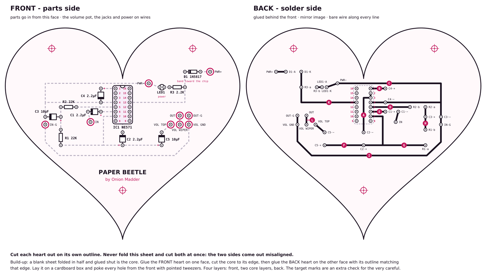
Front: each part is drawn where it sits, with its value printed next to it. The faint dashed lines are only a preview of what connects on the back. The ringed holes are for wires going off the board: PWR+ and PWR− for power; IN and IN-G for the input jack; VOL TOP, VOL WIPER and VOL GND for the volume pot; OUT and OUT-G for the output jack. The three target marks are an extra check for the very careful: on the finished heart they sit on top of each other.
Back: every bold black line is bare wire or a bent part leg. The lines with a letter in a circle are bare wire, and the steps name them by that letter; the short unlettered ones are a part's own leg, bent along the line. Small pink numbers beside the chip holes are its pin numbers. There are no insulated wires on this board.
Steps 1–12 Assembly
tap to expand / collapse
The sheet is the circuit board, four sheets of paper thick: the two printed hearts glued to the two faces of a plain sheet folded in half. Each heart is cut out on its own, and the back lines up with the front by its edge, so there is nothing to fold and nothing to misalign.
Print at 100% / "Actual size". Fit-to-page shrinks it and the holes stop matching the chips' legs.
| Step | Do |
|---|---|
| 1 | Print page 1 on plain printer paper at 100% / Actual size. |
| 2 | Measure the 100 mm bar at the top right of the sheet. If it isn't 100 mm, fix the print scale and print again. |
| 3 | Cut out the FRONT heart along its outline. Then cut out the BACK heart along its own outline. Don't fold the printed sheet and cut both at once: the two sides come out misaligned.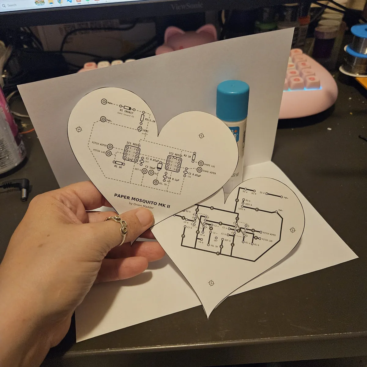 |
| 4 | Fold a second, blank sheet of printer paper in half. Glue-stick the whole inside, close it, and press it flat. That's the core: two sheets thick.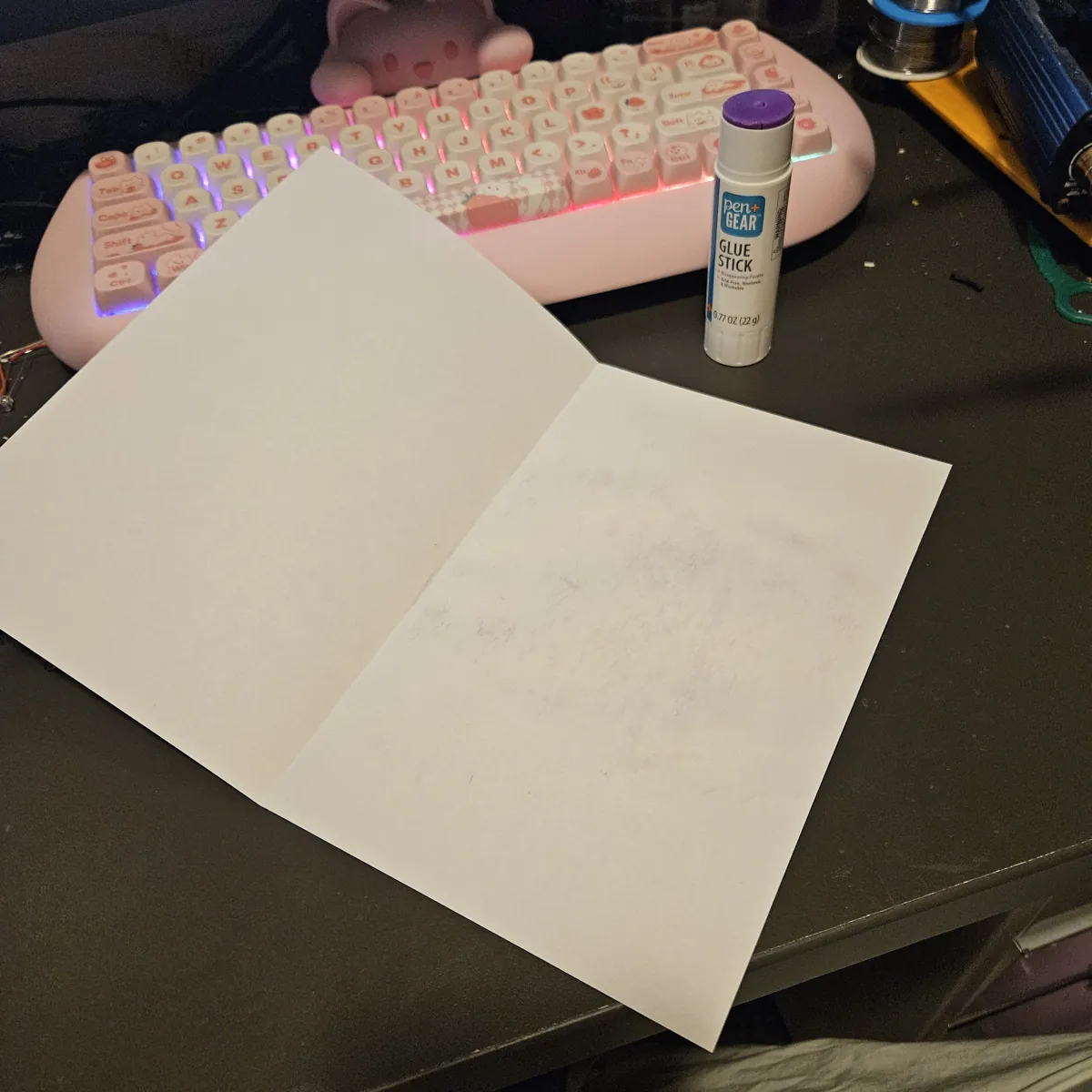 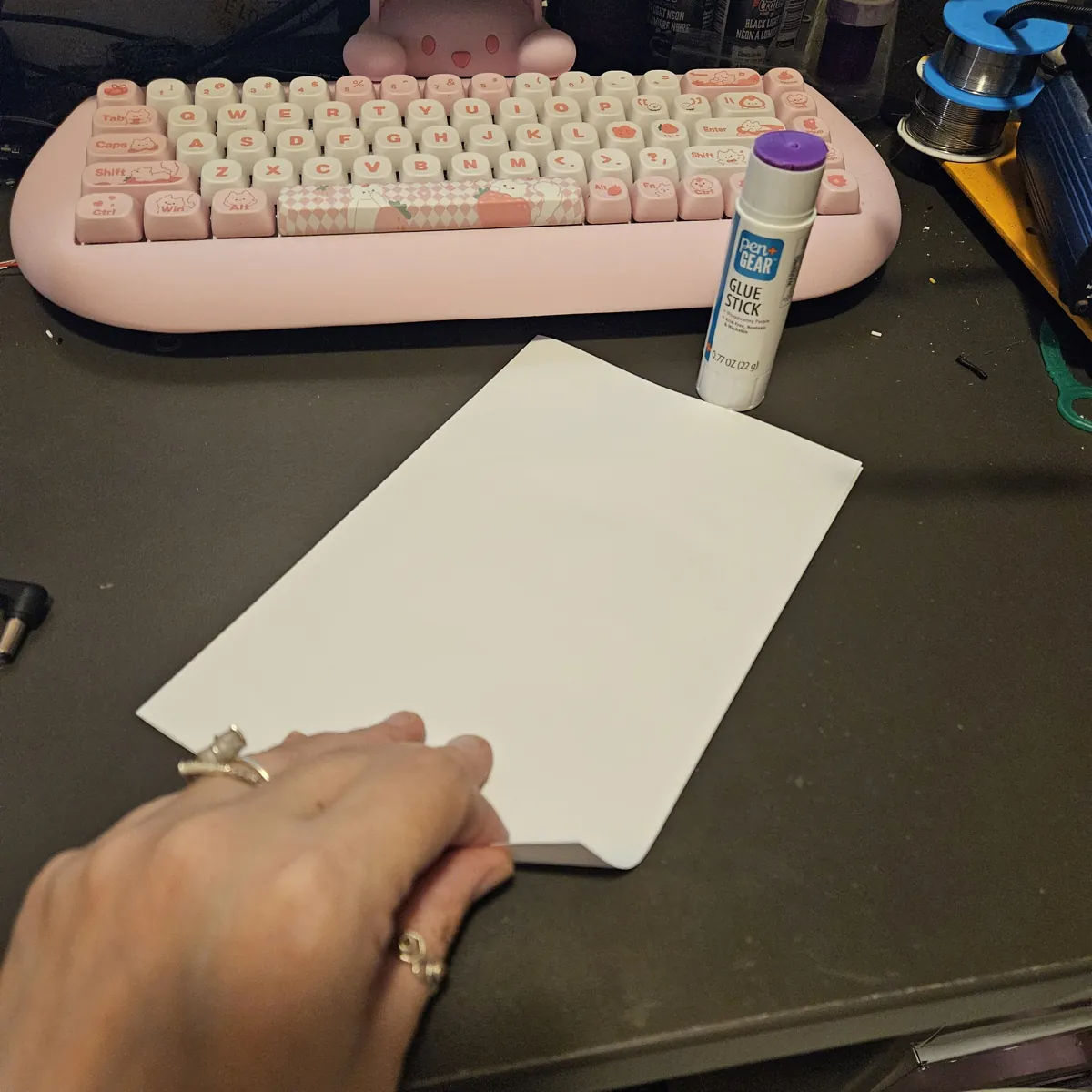 |
| 5 | Glue-stick the back of the FRONT heart.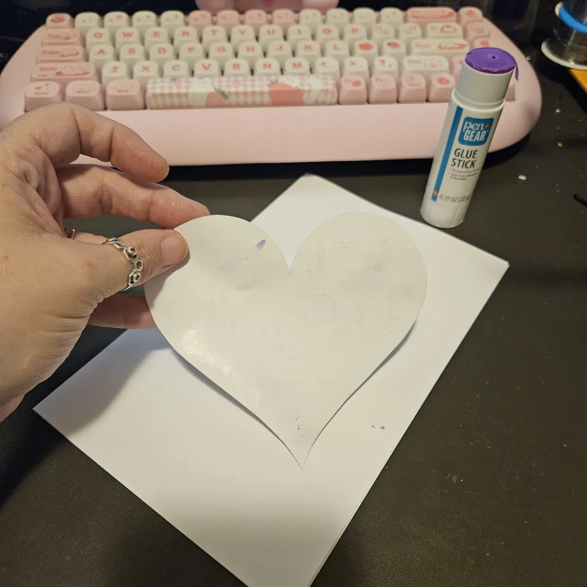 |
| 6 | Press the FRONT heart onto one face of the core, smoothing it flat from the middle out.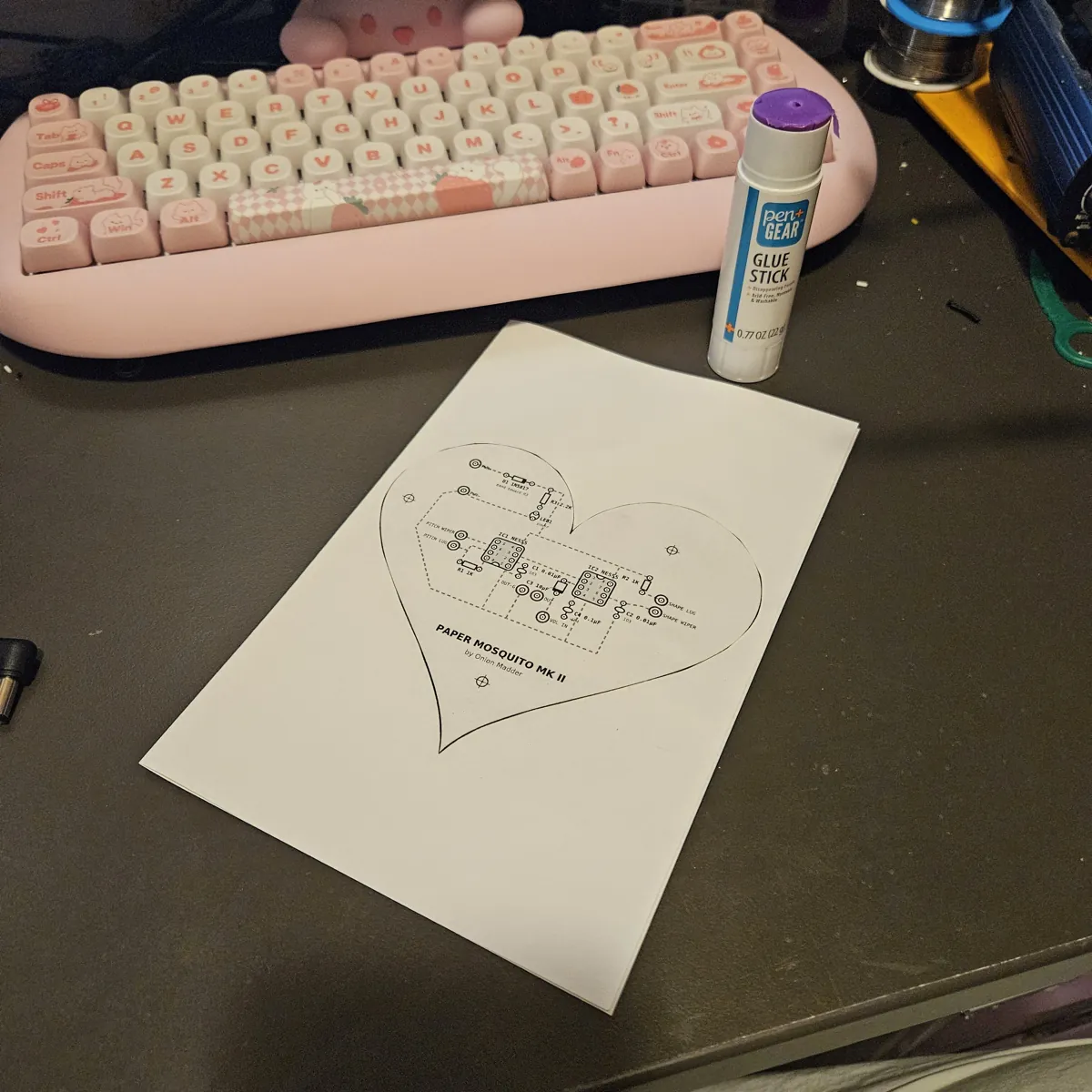 |
| 7 | Cut the core away around the FRONT heart, following its edge, so the core is the same heart shape.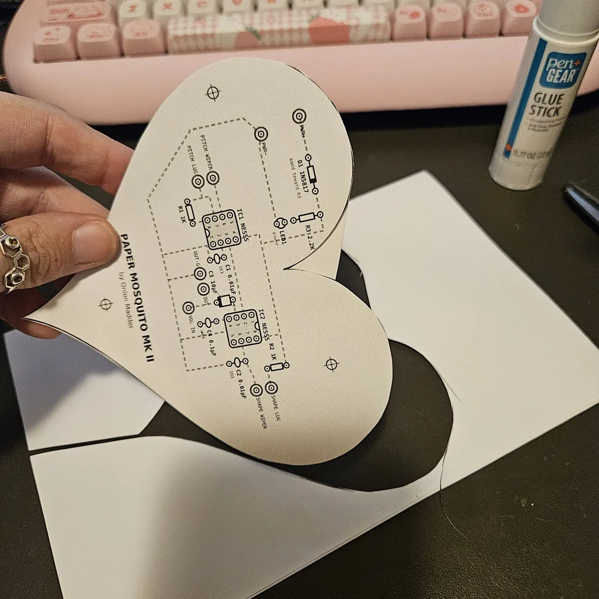 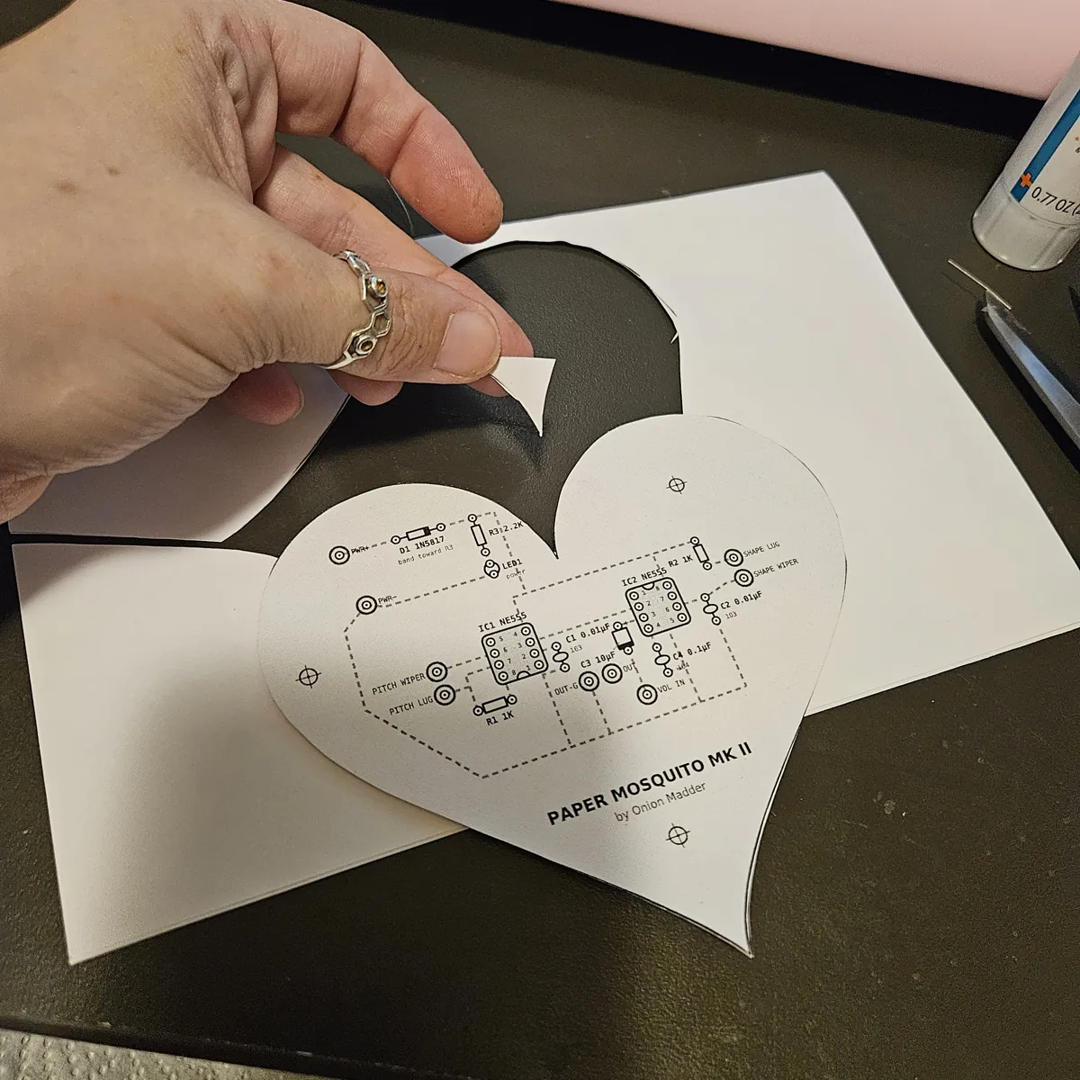 |
| 8 | Glue-stick the bare side of the core.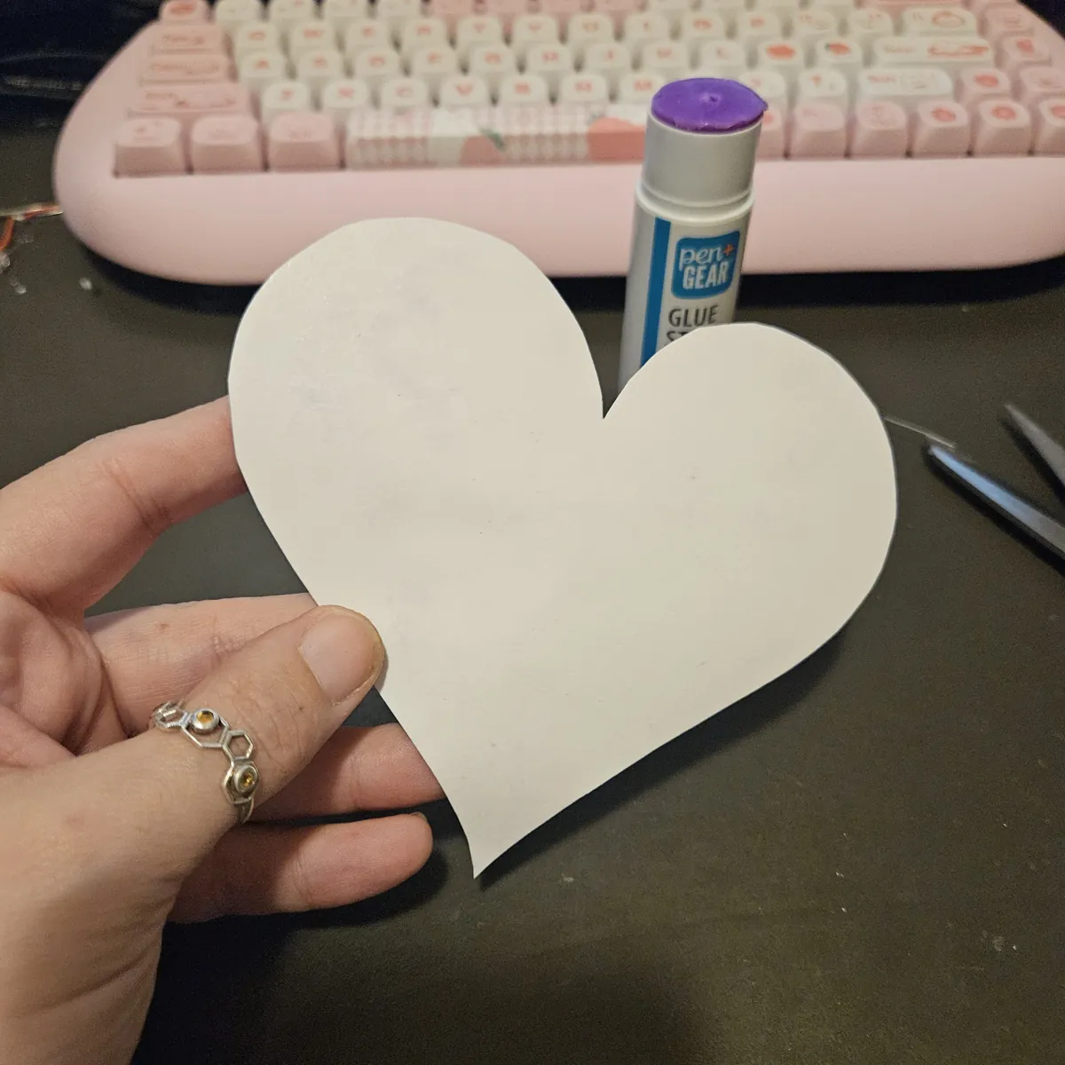 |
| 9 | Lay the BACK heart on it, printed side out, with its outline matching the edge all the way around, and press it flat. Now it's four sheets thick. The 3 target marks are there for the very careful: hold the heart up to a light and the targets on the two sides should sit on top of each other.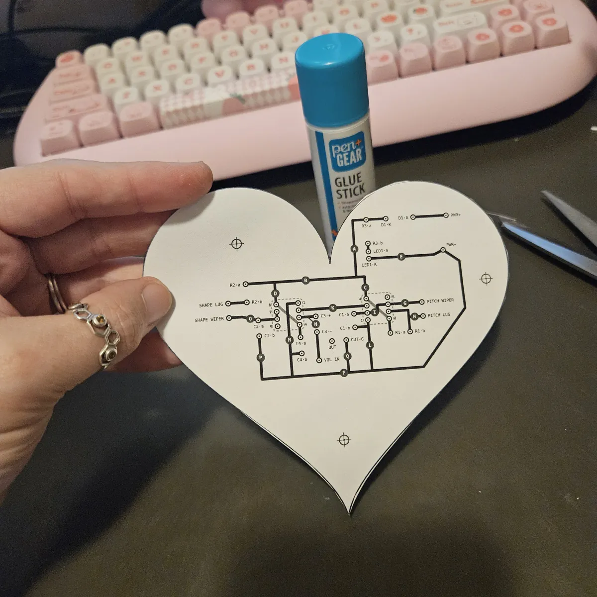 |
| 10 | Let the glue set for a few minutes. Then lay the heart front side up on a cardboard box, and poke the 16 chip holes straight down through all four layers with pointed tweezers, held closed. The box takes the points.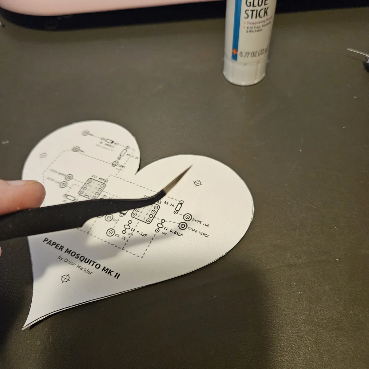 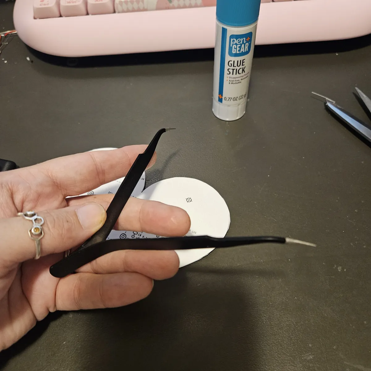 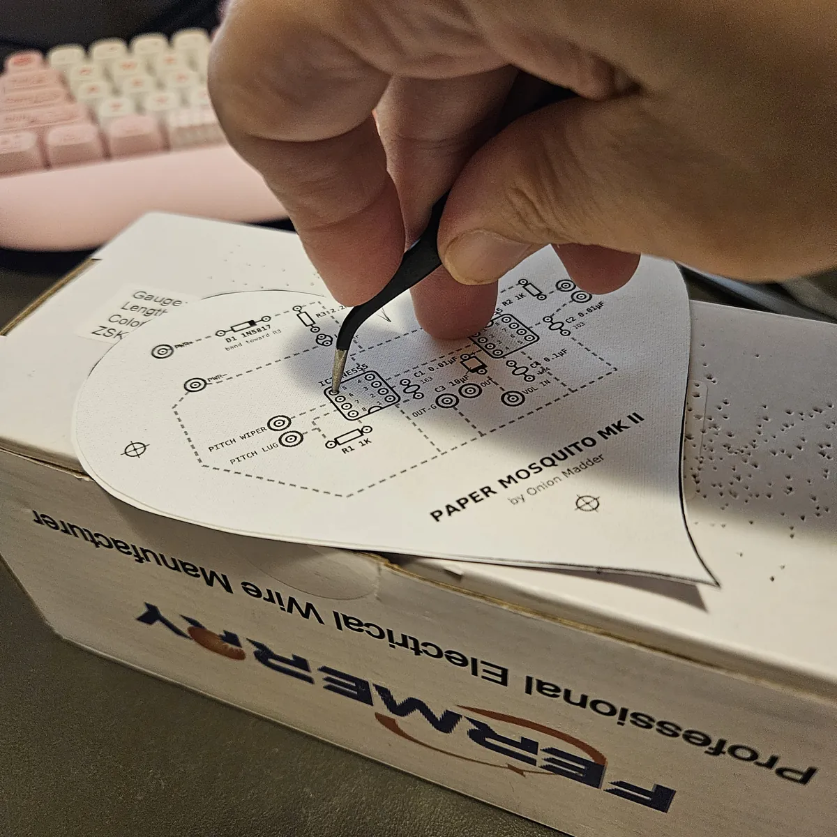 |
| 11 | Poke the other 29 dots and rings the same way. Check the back and open any hole that didn't come all the way through.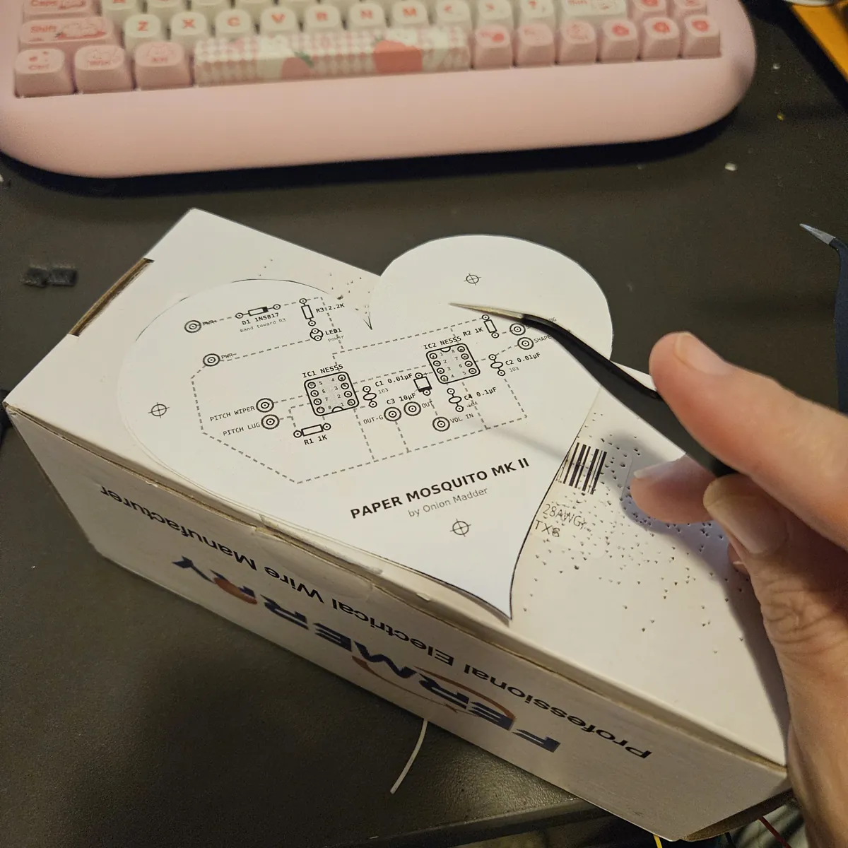 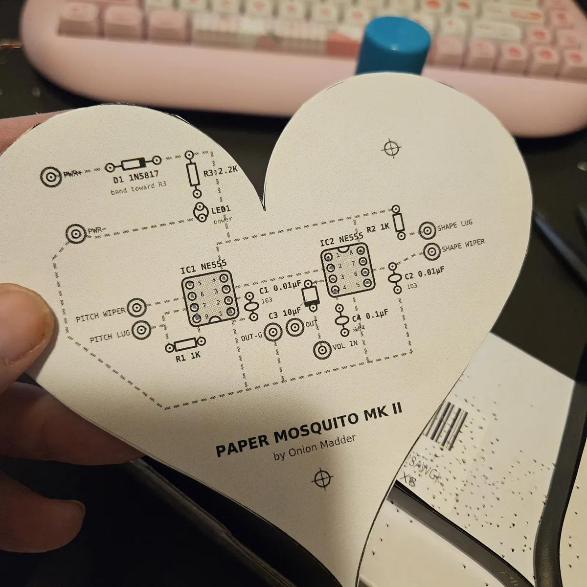 |
| 12 | Check the fit: push each chip into its holes until its legs come through on the back. If a leg won't go, open that hole a little more.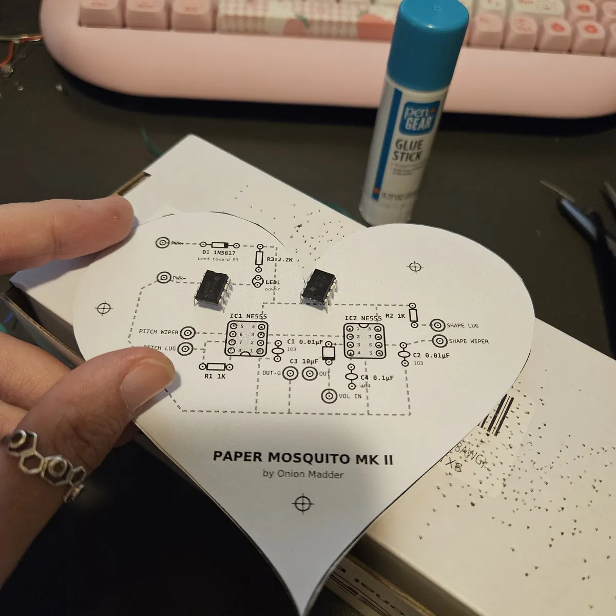 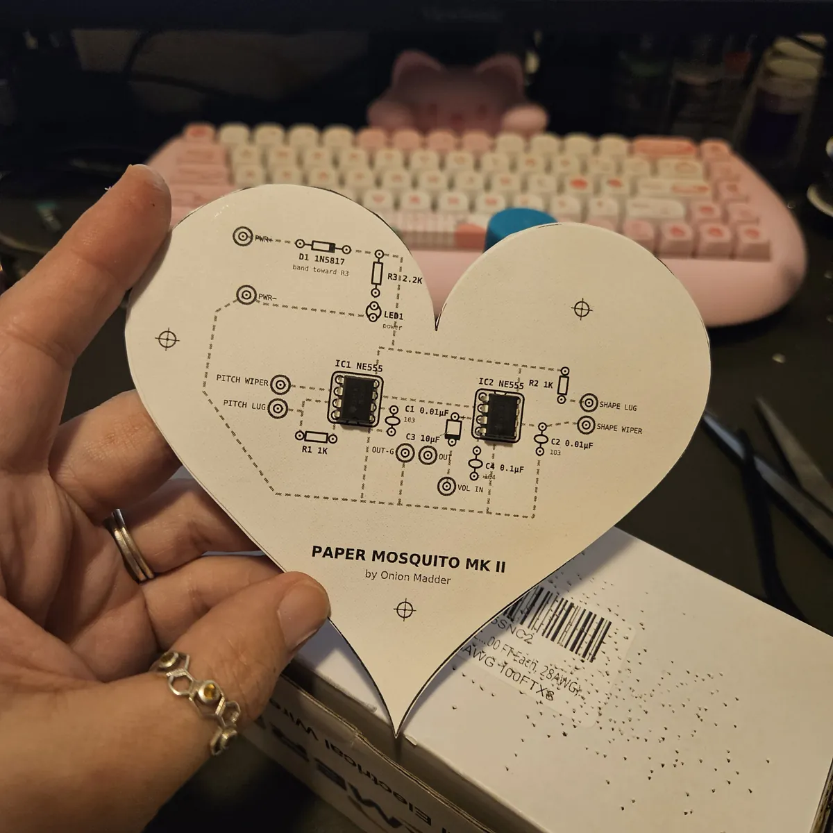 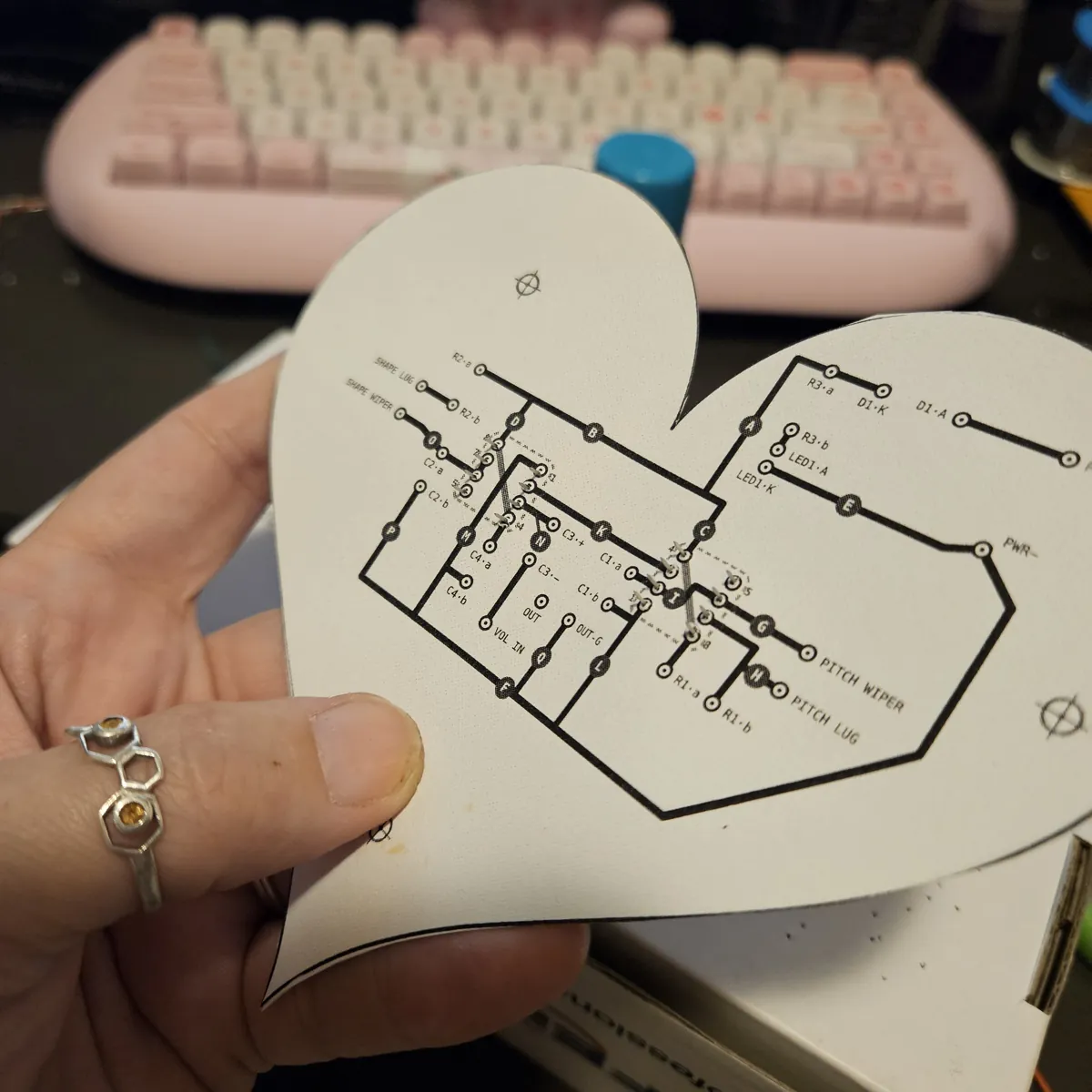 |
Steps 13–16 Start in the middle: the chip and the wire under it
Everything builds outward from the chip. Pins 2 and 3 are joined and go down between the rows, out under the chip to C2.
Quick dabs only. Paper scorches if you sit on it: touch, flow, lift.
| Step | Do |
|---|---|
| 13 | Push the NE571 into the IC1 holes from the front, notch toward the top edge (the drawn notch). |
| 14 | On the back, bend pins 1, 8, 9 and 16 outward slightly so the chip can't fall out. |
| 15 | Trace A: bare wire from pin 2 to pin 3, then a little way in between the rows and straight down past pins 4 to 8 without touching them, out under the chip to the C2·− hole. Solder at pins 2 and 3; the far end gets soldered as C2 goes in. |
| 16 | Check with a meter: trace A must not beep to pins 4, 5, 6, 7 or 8. |
Steps 17–24 The left side: the input, the detector and the DC loop
The input comes in through C1 to pin 6. C4 smooths the chip's level detector. R1, R2 and C3 hold the output at about half the supply without touching the sound.
Every can here has its stripe away from the chip, except C4, whose stripe points down.
| Step | Do |
|---|---|
| 17 | C4, 2.2 µF: long + leg into C4·+ (the top hole, by pin 1), striped leg into C4·−. The − leg gets soldered when trace C goes in. |
| 18 | Trace B: bare wire from pin 1 out to the left to C4·+. Solder at both. |
| 19 | R2, 22K (red-red-orange): legs into R2·a and R2·b. |
| 20 | Trace D: bare wire from pin 5 out to the left to R2·b. Solder at both. |
| 21 | C1, 2.2 µF: long + leg into C1·+ (the hole nearer the chip), striped leg into C1·−. Bend C1·−'s leg down to the IN pad and solder at both. |
| 22 | Trace E: bare wire from pin 6 out to the left to C1·+. Solder at both. |
| 23 | C3, 10 µF: long + leg into C3·+, striped leg into C3·− (the left hole). The − leg gets soldered when trace I goes in. |
| 24 | Trace H: bare wire from R2·a straight down through C3·+ to the R1·b hole. Solder at R2·a and C3·+; R1·b gets soldered as R1 goes in. |
Steps 25–29 Under the chip: the output
Pin 7 is the output. It runs left, down and along under the chip, picking up C2, which feeds it back to pins 2 and 3, and R1, the other half of the DC loop, on the way to C5.
C2's stripe points up, toward the chip; C5's too.
| Step | Do |
|---|---|
| 25 | C2, 2.2 µF: long + leg into C2·+ (the lower hole), striped leg into C2·−, where trace A ends. Solder C2·− to trace A. |
| 26 | R1, 22K: legs into R1·a (the lower hole) and R1·b. Solder R1·b where trace H ends. |
| 27 | C5, 10 µF: long + leg into C5·+ (the lower hole), striped leg into C5·−. Bend C5·−'s leg up to the VOL TOP pad and solder at both. |
| 28 | Trace F: bare wire from pin 7 out to the left, down past C1 and the IN pad, then right along under the chip through C2·+ to C5·+. Solder at pin 7, C2·+ and C5·+. |
| 29 | Trace G: bare wire from the corner of trace F out to the left to R1·a. Solder at R1·a and where it meets F. |
Steps 30–33 Power corner and the +V line
Power comes in on two pads at the top. D1 only lets current through one way, so power hooked up backwards does nothing, and LED1 says it's on.
D1's band goes in D1·K, toward the chip.
| Step | Do |
|---|---|
| 30 | D1, 1N5817: band end into D1·K, plain end into D1·A. Bend D1·A's leg to the PWR+ pad and solder at both. |
| 31 | R3, 2.2K (red-red-red): legs into R3·a and R3·b. |
| 32 | Trace K, +V: bare wire from D1·K straight down through R3·a, then left to pin 13. Solder at D1·K, R3·a and pin 13. |
| 33 | LED1: long leg into LED1·A, short leg into LED1·K. Bend R3·b's leg to LED1·A and solder at both. Bend LED1·K's leg to the PWR− pad and solder at both. |
Steps 34–37 The ground line
Ground runs from pin 4 out to the left, up and over the top of the chip to PWR−, and from the left side down and along the bottom to the jack and volume pads.
| Step | Do |
|---|---|
| 34 | Trace C, ground: bare wire from pin 4 out to the left through C4·−, up the left side and over the top of the chip to the PWR− pad. Solder at pin 4, C4·− and PWR−. |
| 35 | Trace I: bare wire from trace C's corner on the left, down through C3·− and the IN-G pad, along the bottom of the heart and up the right side through the VOL GND pad to the OUT-G pad. Solder where it meets C, at C3·−, IN-G, VOL GND and OUT-G. |
| 36 | Trace L: bare wire from the VOL WIPER pad up to the OUT pad. Solder at both. |
| 37 | Snip every leg tail that sticks past its joint. |
Steps 38–41 Off the board
The volume pot, the two jacks, the toggle and the power hang off the pads on insulated wire.
If the volume knob feels backwards, swap its two outer wires.
| Step | Do |
|---|---|
| 38 | Volume pot: one outer lug to VOL TOP, the middle lug to VOL WIPER, the other outer lug to VOL GND. No pot? A short wire from VOL TOP to VOL WIPER and it plays at full volume. |
| 39 | Input jack tip to IN, sleeve to IN-G. Output jack tip to OUT, sleeve to OUT-G. |
| 40 | A wire from one lug of the power toggle to the PWR+ pad. |
| 41 | Battery: the snap's red (+) wire to the toggle's other lug, its black (−) wire to PWR−. Or a DC jack for a center-negative 9V pedal supply: the jack's sleeve (+) lug to the toggle's other lug, its center-pin (−) lug to PWR−. |
Steps 42–44 Check, then play
Meter it before you play it. These readings come from the datasheet and arithmetic, not off my board.
| Step | Do |
|---|---|
| 42 | Turn the volume down. Toggle on: LED1 should light. |
| 43 | Meter pin 13 to pin 4: the supply voltage minus about 0.3 V. Pins 2, 3, 5 and 6 to pin 4: about 1.8 V each, the chip's own reference. Pin 7 to pin 4: about 4.4 V. |
| 44 | Plug a guitar or another pedal into IN and bring the volume up. Play soft, then hard: the hard notes should come out not much louder than the soft ones, and a held chord should hang on longer than it does dry. |
⚠ If it won't sing
| Meter between | EXPECT (toggle on, nothing plugged in) |
|---|---|
| PWR+ pad → PWR− pad | supply voltage |
| pin 13 → pin 4 | supply voltage minus about 0.3 V |
| pins 2, 3, 5 and 6 → pin 4 | about 1.8 V, the chip's reference, whatever the supply |
| pin 7 → pin 4 | about 4.4 V, set by R1 and R2 |
| Symptom | Check |
|---|---|
| Dead, LED1 dark | D1 in backwards (the band goes in D1·K), the power wires reversed, or the toggle not between the supply's + and PWR+. |
| LED1 lit, silent | Pin 7 should read about 4.4 V. Near 0 V or near the supply: R1, R2, trace H and trace D. Then C5 to VOL TOP, the volume pot, and C1 to IN. |
| Loud and distorted, no squeeze | The detector is not seeing the output: C2 and trace A to pins 2 and 3. Pins 2 and 3 should read 1.8 V. |
| Pumps or flutters on low notes | C4 is too small for the lowest notes. Try 4.7 µF or 10 µF in its place: slower, smoother. |
| Dull with a guitar straight in | The input is the chip's own 20K, lower than most pedals. Put a buffer or another pedal before it. |
| Paper scorched or a hole tore | Glue a scrap of paper over the back, re-poke, carry on. It is paper. |
Built, and heard
It sounds really great. I don’t know what it’s supposed to sound like, but it gets loud and crunchy and gives a nice big gnarly sound.
Things to try
- A slower squeeze. C4 at 10 µF smooths the detector about four and a half times longer, for a gentler swell. Untried.
- After a fuzz. A compressor after a fuzz evens out its sputter on a fading note. Untried.
- On a drum machine or a synth, to pull its quiet hits up to its loud ones. Untried.
The circuit is the Basic Compressor from onsemi's NE570 datasheet, the NE571's sibling with the same pins. The paper-circuit method is Peter Blasser's / Ciat-Lonbarde's. This layout and the words are my own, and so is anything wrong with them.