Paper Ring Mod
A one-chip ring modulator as a heart-shaped paper circuit · By Onion Madder · Mess O' Pedals
A ring modulator on paper: plug two oscillators into it and it smashes them together. Each input is squared up by a gate of its own, so it is drawn to take the other paper builds straight from their jacks, and an XOR gate multiplies the two. One CD4070, one volume knob, and the jacks and power on wires.
⚠ Before you start tap to expand / collapse
Paper burns. Keep the iron moving, quick joints, and don't rest it on the sheet. Work over something that isn't flammable, and keep a damp sponge handy.
Chip straight in. The CD4070 is soldered straight to the paper with no socket, and four bare wires run between its two rows of legs on the back. Keep each joint quick: touch, flow, lift.
Mind the cans. C3 and C4 are polarized: the stripe is the − leg, and the sheet marks each + hole.
1M is not 100K. R3 and R6 are brown-black-green; the four 100Ks are brown-black-yellow. Swapped, an input needs a much louder signal to do anything.
What you'll need
tap to expand / collapse
New to the parts? Each line notes how to spot it - the printed marking, the package, or the polarity clue.
- 1× CD4070 quad XOR (IC1) - spot it: CD4070 printed on top, notch or dot at pin 1, 14 pins. A CD4030 is the same chip under an older number. It solders straight to the paper, no socket.
- 4× 100K resistors (R1, R4, R7, R8) - spot it: brown-black-yellow. R7 and R8 make half the supply; R1 and R4 hang each input on it.
- 2× 10K resistors (R2, R5) - spot it: brown-black-orange. One in front of each input gate.
- 2× 1M resistors (R3, R6) - spot it: brown-black-green. The feedback that gives each input its snap: don't swap them with the 100Ks.
- 3× 0.1 µF ceramic (C1, C2, C5) - spot it: printed 104. C1 and C2 couple the inputs; C5 sits across the supply at the chip.
- 2× 10 µF electrolytic (C3, C4) - spot it: a little can, stripe marks the − leg. C3 holds the half supply still; C4 is the output's DC blocker.
- 1× 1N5817 Schottky diode (D1) - spot it: small black body, gray or silver band marks the cathode
- 1× LED (LED1) and a 2.2K resistor (R9) - spot it: the power light. The LED's long leg is +, the flat side of the rim −; 2.2K is red-red-red
- 1× A100K pot (volume) - spot it: marked A100K; A = log, the right taper for volume. It hangs off the board on wires, so any style fits.
- 1× SPST toggle - spot it: for power; it hangs off the board on wires
- 3× jacks - spot it: two inputs and the output, on wires
- Bare tinned wire, and insulated wire - spot it: bare for the traces on the back, insulated for every wire off the board
- Power: a 9V battery and snap, or a 2.1 mm DC jack and a 9V pedal supply - spot it: the usual pedal supply is center-negative
- A second sheet of plain printer paper, a glue stick, scissors, pointed tweezers and a cardboard box - spot it: the blank sheet becomes the core; the tweezers poke the holes and the box takes the points
Quick reference - the chip
The chip sits on the sheet exactly like this, notch toward the top edge. Gate 1 squares input A, gate 4 squares input B, and gate 2 is the XOR of the two. Gate 3 is spare: pin 8 is grounded, pin 9 rides on input B's line so it never floats, and pin 10 stays empty on purpose.
Reading the sheet
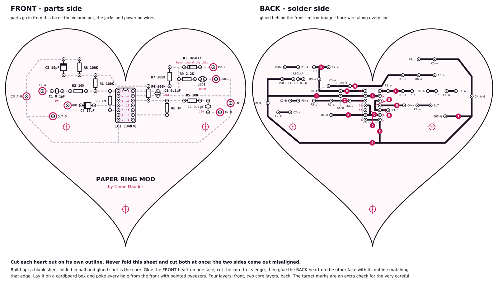
Front: each part is drawn where it sits, with its value printed next to it. The faint dashed lines are only a preview of what connects on the back. The ringed holes are for wires going off the board: PWR+ and PWR− for power; IN A and IN A-G, IN B and IN B-G for the two input jacks; OUT and OUT-G for the volume pot. The three target marks are an extra check for the very careful: on the finished heart they sit on top of each other.
Back: every bold black line is bare wire or a bent part leg. The lines with a letter in a circle are bare wire, and the steps name them by that letter; the short unlettered ones are a part's own leg, bent along the line. Small pink numbers beside the chip holes are its pin numbers. Four of the lettered wires run between the chip's two rows of legs: that is on purpose, and the steps say which pins each one touches.
Steps 1–12 Assembly
The sheet is the circuit board, four sheets of paper thick: the two printed hearts glued to the two faces of a plain sheet folded in half. Each heart is cut out on its own, and the back lines up with the front by its edge, so there is nothing to fold and nothing to misalign.
Print at 100% / "Actual size". Fit-to-page shrinks it and the holes stop matching the chips' legs.
| Step | Do |
|---|---|
| 1 | Print page 1 on plain printer paper at 100% / Actual size. |
| 2 | Measure the 100 mm bar at the top right of the sheet. If it isn't 100 mm, fix the print scale and print again. |
| 3 | Cut out the FRONT heart along its outline. Then cut out the BACK heart along its own outline. Don't fold the printed sheet and cut both at once: the two sides come out misaligned. |
| 4 | Fold a second, blank sheet of printer paper in half. Glue-stick the whole inside, close it, and press it flat. That's the core: two sheets thick. |
| 5 | Glue-stick the back of the FRONT heart. |
| 6 | Press the FRONT heart onto one face of the core, smoothing it flat from the middle out. |
| 7 | Cut the core away around the FRONT heart, following its edge, so the core is the same heart shape. |
| 8 | Glue-stick the bare side of the core. |
| 9 | Lay the BACK heart on it, printed side out, with its outline matching the edge all the way around, and press it flat. Now it's four sheets thick. The 3 target marks are there for the very careful: hold the heart up to a light and the targets on the two sides should sit on top of each other. |
| 10 | Let the glue set for a few minutes. Then lay the heart front side up on a cardboard box, and poke the 14 chip holes straight down through all four layers with pointed tweezers, held closed. The box takes the points. |
| 11 | Poke the other 40 dots and rings the same way. Check the back and open any hole that didn't come all the way through. |
| 12 | Check the fit: push each chip into its holes until its legs come through on the back. If a leg won't go, open that hole a little more. |
Steps 13–26 Start in the middle: the chip and the wires under it
Everything builds outward from the chip. Four bare wires run on the back between its two rows of legs, and the rest run out from its pins. Solder each at its pins now, and the holes along it as their parts go in.
Quick dabs only. Paper scorches if you sit on it: touch, flow, lift.
| Step | Do |
|---|---|
| 13 | Push the CD4070 into the IC1 holes from the front, notch toward the top edge (the drawn notch). |
| 14 | On the back, bend pins 1, 7, 8 and 14 outward slightly so the chip can't fall out. |
| 15 | Trace A: bare wire straight across between the rows, from pin 2 to pin 13. Solder at both. That is ground for two of the spare inputs. |
| 16 | Trace E: bare wire straight across from pin 8 to pin 7, then down to the ground line. Solder at pin 8 and pin 7; the far end gets soldered with the line. |
| 17 | Trace B: bare wire from pin 3 a little way in between the rows, down past pin 4 without touching it, and back out to pin 5. Solder at pin 3 and pin 5. |
| 18 | Trace D: bare wire straight across from pin 9 to pin 6. Solder at both. |
| 19 | Trace C: bare wire from pin 11 a little way in between the rows, then down past pin 10 without touching it to meet trace D. Solder at pin 11 and where it meets D. |
| 20 | Check with a meter before going on: pin 4 and pin 10 must not beep to anything. Those are the two pins the wires go around. |
| 21 | Trace F: bare wire from pin 1 out to the left, to the R2·b hole. Solder at pin 1. |
| 22 | Trace G: bare wire from pin 4 out to the left, to the C4·+ hole. Solder at pin 4. |
| 23 | Trace H: bare wire from pin 5 out to the left, to the R3·b hole. Solder at pin 5. |
| 24 | Trace I: bare wire from pin 12 out to the right, to the R5·b hole. Solder at pin 12. |
| 25 | Trace K: bare wire from pin 9 out to the right, to the R6·b hole. Solder at pin 9. |
| 26 | Trace O: bare wire from pin 13 out to the right, all the way to the right ground line. Solder at pin 13 only; the far end gets soldered with the line. |
Steps 27–31 The left side: input A and the output
Input A comes in through C1 and R2 to pin 1. R1 hangs pin 1 on the half supply, and R3 from pin 3's line gives it its snap. Pin 4 is the sound; it goes through C4 to OUT.
| Step | Do |
|---|---|
| 27 | C1, 0.1 µF (104): legs into C1·a and C1·b. Bend C1·a's leg to the IN A pad and solder at both. |
| 28 | R2, 10K (brown-black-orange): legs into R2·a and R2·b. Bend C1·b's leg to R2·a and solder at both. Solder R2·b where trace F ends. |
| 29 | R1, 100K (brown-black-yellow): legs into R1·a and R1·b. Solder R1·a on trace F. R1·b waits for the VREF line. |
| 30 | R3, 1M (brown-black-green): legs into R3·a and R3·b. Solder R3·a on trace F and R3·b where trace H ends. |
| 31 | C4, 10 µF: long + leg into C4·+, striped leg into C4·−. Solder C4·+ where trace G ends. Bend C4·−'s leg to the OUT pad and solder at both. |
Steps 32–35 The right side: input B
Input B is the mirror image: C2 and R5 to pin 12, R4 to the half supply, R6 from pin 9's line for the snap.
| Step | Do |
|---|---|
| 32 | C2, 0.1 µF (104): legs into C2·a and C2·b. Bend C2·a's leg to the IN B pad and solder at both. |
| 33 | R5, 10K (brown-black-orange): legs into R5·a and R5·b. Bend C2·b's leg to R5·a and solder at both. Solder R5·b where trace I ends. |
| 34 | R4, 100K: legs into R4·a and R4·b. Solder R4·a on trace I. R4·b waits for the VREF line. |
| 35 | R6, 1M (brown-black-green): legs into R6·a and R6·b. Solder R6·a on trace I and R6·b where trace K ends. |
Steps 36–39 The half supply over the top
R7 and R8 split the supply in half, C3 holds it still, and the VREF line carries it to R1 and R4.
C3's stripe goes toward the top edge.
| Step | Do |
|---|---|
| 36 | C3, 10 µF: long + leg into C3·+, striped leg into C3·−. |
| 37 | R8, 100K: legs into R8·a and R8·b. |
| 38 | R7, 100K: legs into R7·a and R7·b. |
| 39 | Trace Q, the VREF line: bare wire from C3·+ along over the top of the chip to R7·b. Solder at C3·+, R8·a, R1·b, R4·b and R7·b. |
Steps 40–45 Power corner and the +V line
Power comes in on two pads at the top right. D1 only lets current through one way, so power hooked up backwards does nothing; C5 steadies the supply at the chip and the LED says it's on.
D1's band goes in D1·K, toward the chip.
| Step | Do |
|---|---|
| 40 | D1, 1N5817: band end into D1·K, plain end into D1·A. Bend D1·A's leg to the PWR+ pad and solder at both. |
| 41 | Trace N: bare wire from R7·a across to D1·K. Solder at both. |
| 42 | Trace M, the +V line: bare wire from pin 14 out to the right, then up to meet trace N. Solder at pin 14 and where it meets N. |
| 43 | C5, 0.1 µF (104): legs into C5·a and C5·b. Solder C5·a on trace M and C5·b on trace O. |
| 44 | R9, 2.2K (red-red-red): legs into R9·a and R9·b. Solder R9·a on trace M. |
| 45 | LED1: long leg into LED1·A, short leg into LED1·K. Bend R9·b's leg to LED1·A and solder at both. Bend LED1·K's leg to the PWR− pad and solder at both. |
Steps 46–48 The ground line
One ground wire runs from R8 and C3 in the left lobe, down the left side, along the bottom and up the right side to PWR−, and everything that goes to ground drops onto it.
| Step | Do |
|---|---|
| 46 | Trace S, ground: bare wire from R8·b left through C3·−, down the left side through the IN A-G pad, along the bottom, up the right side through the IN B-G pad, to PWR−. Solder at every pad and part leg on it, and where traces E and O meet it. |
| 47 | Trace T: bare wire from the OUT-G pad across to the left ground line. Solder at OUT-G and where it meets S. |
| 48 | Snip every leg tail that sticks past its joint. |
Steps 49–53 Off the board
The volume pot, the jacks, the toggle and the power hang off the pads on insulated wire.
If the volume knob feels backwards, swap its two outer wires.
| Step | Do |
|---|---|
| 49 | Volume pot: one outer lug to OUT, the other outer lug to OUT-G, and the middle lug to the output jack's tip. |
| 50 | Output jack sleeve to OUT-G. |
| 51 | Input A jack: tip to IN A, sleeve to IN A-G. Input B jack: tip to IN B, sleeve to IN B-G. |
| 52 | A wire from one lug of the power toggle to the PWR+ pad. |
| 53 | Battery: the snap's red (+) wire to the toggle's other lug, its black (−) wire to PWR−. Or a DC jack for a center-negative 9V pedal supply: the jack's sleeve (+) lug to the toggle's other lug, its center-pin (−) lug to PWR−. |
Steps 54–57 Check, then play
Meter it before you play it. These readings are with the chip in and nothing plugged into the inputs. They are arithmetic, not measurements from a built board.
| Step | Do |
|---|---|
| 54 | Clip the battery on or plug the supply in, and toggle on. LED1 should light. |
| 55 | Meter pin 14 to pin 7: the supply voltage minus about 0.3 V. Meter R7·b to pin 7: about half of that. |
| 56 | Turn the volume down and plug one oscillator into IN A, its volume up. Bring the volume up slowly: you should hear that oscillator on its own, squared up. |
| 57 | Plug a second oscillator into IN B. Now the two smash together: sweep one and hold the other still. |
⚠ If it won't sing
| Meter between | EXPECT (toggle on, nothing plugged in) |
|---|---|
| PWR+ pad → PWR− pad | supply voltage |
| pin 14 → pin 7 | supply voltage minus about 0.3 V |
| R7·b → pin 7 | half of pin 14, about 4.3 V on a fresh 9 V |
| pin 1 → pin 7, and pin 12 → pin 7 | within about half a volt of R7·b, one side or the other, and steady |
| pin 4 → pin 7 | zero, or the full supply; steady either way |
| Symptom | Check |
|---|---|
| Dead, LED dark | D1 in backwards (the band goes in D1·K), the power wires reversed, or the toggle not between the supply's + and PWR+. |
| LED lit, silent with one input plugged in | The source's own volume: it wants a couple of volts. Then trace G and C4 to OUT, and the volume pot: one outer lug on OUT, the other on OUT-G, the wiper to the jack tip. |
| One input works, the other does nothing | Compare its side with the side that works: the coupling cap, the 10K, the 1M feedback resistor and the 100K to the VREF line. R7·b should read half the supply. |
| Both inputs come through mixed, not smashed | Pin 4's line and pin 10 must not touch anything else: traces B and C go around them between the rows. Then traces A and D. |
| A quiet source drops in and out | It is on the edge of switching the input. Turn the source up, or try 2.2M in that side's feedback resistor (untested). |
| Paper scorched or a hole tore | Glue a scrap of paper over the back, re-poke, carry on. It is paper. |
Things to try
- Two of the other paper builds into it. A Paper Mosquito Mk II on one input and a Paper Dragonfly on the other, with their volumes up, and sweep one while the other holds still. Untried, like everything here.
- One input only: the empty side sits still, so you hear the other input squared up, which is a fuzz of sorts on its own.
- Close pitches: two oscillators nearly in tune give a difference tone slow enough to hear as a beat.
- Change the snap: R3 and R6 at 470K make the inputs harder to flip, so a quiet source drops out; at 2.2M they flip more easily and a slow wave may chatter at the edges.
An XOR as a ring modulator for square waves is the standard Lunetta trick, and a gate with feedback as a Schmitt trigger is out of every CMOS cookbook. The paper-circuit method is Peter Blasser's / Ciat-Lonbarde's. This layout and the words are my own, and so is anything wrong with them.