XOR Ring Mod
Two inputs, one chip, one knob · By Onion Madder · Mess O' Pedals
Plug two oscillators into it and it smashes them together. An XOR gate is a ring modulator for square waves: its output is high only when its two inputs disagree, and that is the same thing as multiplying two square waves, so out comes the sum and the difference of the two pitches. This is that gate with a front end on each input that squares up whatever you feed it, so it is drawn to take the outputs of the other builds on this site straight from their jacks. One CD4070 does all of it, on a 12 by 22 board.
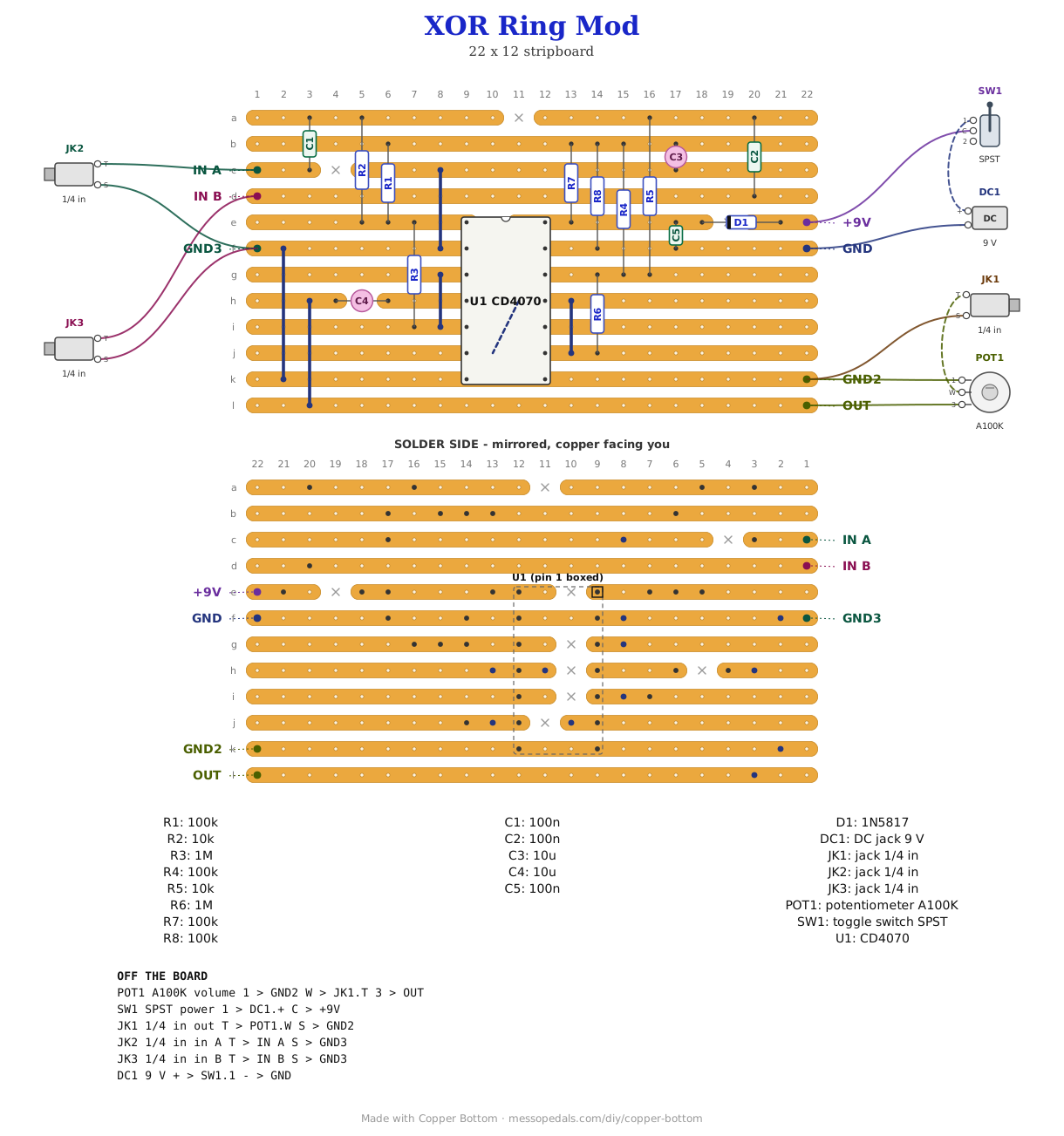
What you'll need
tap to expand / collapse
Fourteen parts on the board plus the chip and six links, and six off it.
- 1× CD4070 quad XOR, DIP-14 (U1) - spot it: fourteen legs, the number printed on top, a notch at one end. A CD4030 is the same thing under an older number. Three gates are used and the fourth is tied off. It solders straight to the board
- 1× 1N5817 Schottky (D1) - spot it: fat black body, a gray band at one end. Reverse-polarity protection on the supply; the band goes toward the chip
- 4× 100K resistor (R1, R4, R7, R8) - spot it: bands brown-black-yellow. R7 and R8 make half the supply; R1 and R4 hang each input on it
- 2× 10K resistor (R2, R5) - spot it: bands brown-black-orange. One in front of each input gate
- 2× 1M resistor (R3, R6) - spot it: bands brown-black-green. The feedback that gives each input its snap. Do not swap them with the 100Ks
- 3× 100nF ceramic (C1, C2, C5) - spot it: printed 104. C1 and C2 couple the two inputs; C5 sits across the supply
- 2× 10 µF electrolytic (C3, C4) - spot it: a small can with a stripe down one side; the stripe leg is the negative one. C3 holds the half supply still, stripe to ground. C4 is the output cap, stripe away from the chip
- 6× wire links - offcuts of component leg. One of them, J5, runs diagonally under the chip's body, so it goes in before the chip does
Off the board
- 1× A100K log pot - volume. Lug 3 to OUT, lug 1 to GND2, wiper to the output jack tip. The output is a full-swing square wave, so you will want it
- 3× 1/4 inch jacks - in A and in B on the left, out on the right. Input tips to IN A and IN B, both input sleeves to GND3; output tip to the volume wiper, sleeve to GND2
- 1× DC jack, 9 V center negative
- An SPST toggle for power, in the positive supply lead between the DC jack and the board's +9V pad. Every build on this shelf gets one, and the drawing above shows it
The layout file is the guide
Like every layout on this shelf, the build document for this one is the file itself: ↓ Download XOR_Ring_Mod.json - import it into Copper Bottom and the editor gives you the board picture, the placement walkthrough, the electrical checks and a printable build sheet, all from the same file. No coordinates are written out on this page on purpose: the editor is the viewer, and a number typed twice is a number that can drift.
Both inputs come in on the left and the output leaves on the right, the way the jacks go on my boxes. Input B reaches the left edge along strip d, and the output reaches the right edge along strip l. J5 is the one link under the chip: it carries input B's squared signal from pin 11 across to pin 6, diagonally between the pin rows, and it has to be soldered in before the chip.
The netlist
My script wrote this from the design and the board was checked against it in Copper Bottom: every connection it names is on the board and nothing on the board is missing from it. GA and GB are the two input gates, QA and QB their squared outputs, and MIX is the XOR of the two. Pin 10 is the spare gate's output and is left empty, which is why it is not listed.
The off-board wiring
Six pads leave the board: two inputs and their ground, the output and its ground, and the supply.
| Pad | Goes to |
|---|---|
| IN A / IN B | The two input jack tips. Anything with a wave on it: the output of another build, a synth, a drum machine. Turn the source up; see below for how loud |
| GND3 | Both input jack sleeves |
| OUT | Volume pot lug 3. The wiper goes to the output jack tip, and lug 1 to GND2 |
| GND2 | Volume pot lug 1 and the output jack sleeve. Same net as GND |
| +9V / GND | The supply, through the power toggle. DC jack positive to the toggle and the toggle to +9V; negative to GND |
How it works, in one breath
An XOR gate only understands high and low, so each input first goes through a gate of its own that decides which one it is. C1 blocks whatever DC the source carries, R2 feeds pin 1, and R1 hangs pin 1 on half the supply, which R7 and R8 make and C3 holds still. R3 runs from that gate's output back to its input, and because the gate does not invert, the feedback pushes the way the output already went: by the arithmetic the input has to move about 0.4 V past the middle before the gate flips, and the same back the other way. That is what makes a ragged or slow wave come out as a clean square, and it is why an unplugged input sits still instead of buzzing. Input B gets the same treatment from R5, R4 and R6 on pins 13 and 11.
The two clean squares meet in the third gate, pins 5 and 6, and its output on pin 4 is high only when they disagree. Flipping one square wave in step with another is multiplying them, so what comes out is the sum and the difference of the two pitches and their harmonics, and neither original on its own. C4 takes the DC off, and the volume pot sets how much leaves. The fourth gate does nothing: pin 8 is tied to ground and pin 9 rides along on input B's signal, so neither of its inputs is left floating.
The front end wants a swing of roughly 1 V each way from the middle, about 2 V peak to peak, to switch reliably. That is arithmetic, and the CD4070's own switching point is only promised to land somewhere in the middle third of the supply, so a particular chip may want more. The builds on this site put out a square wave as big as their supply, so with their volume up there is plenty.
Things to try
None of these have been tried, because none of this has. They are the obvious knobs.
- Two of the other builds into it. A Mosquito 556 on one input and a Dragonfly VCO on the other, and sweep one while the other holds still
- One input only. The empty side sits still, so you hear the other input squared up, which is a fuzz of sorts on its own
- Close pitches. Two oscillators nearly in tune give a difference tone that is slow enough to hear as a beat
- Change the snap. R3 and R6 at 470K make the inputs harder to flip, so a quiet source drops out; at 2.2M they flip more easily and a slow wave may chatter at the edges
An XOR as a ring modulator for square waves is the standard Lunetta trick and belongs to everyone who has ever built one, and a gate with feedback as a Schmitt trigger is out of every CMOS cookbook. Putting both on one chip, and the layout, are mine and so is anything wrong with them.