Cicada NAND Mk II
Four gated CD4093 voices, an XOR on every one · By Onion Madder · Mess O' Pedals
The Cicada NAND, grown into a fuller box. The same four voices on one CD4093, each with its own pitch knob and a timing cap a decade from its neighbor, but now the voices can work on each other. Every voice has a gate toggle that turns it off, lets it run, or hands its gate to another voice so that one chops it. Every voice has an XOR toggle that swaps it for the XOR of itself and that same partner. Every gate has a jack, so something else can play it. Then tone, volume and a power light. Two chips on a 22 by 28 board.
The first board is four drones that never meet until the mix. This one is wired so they can.
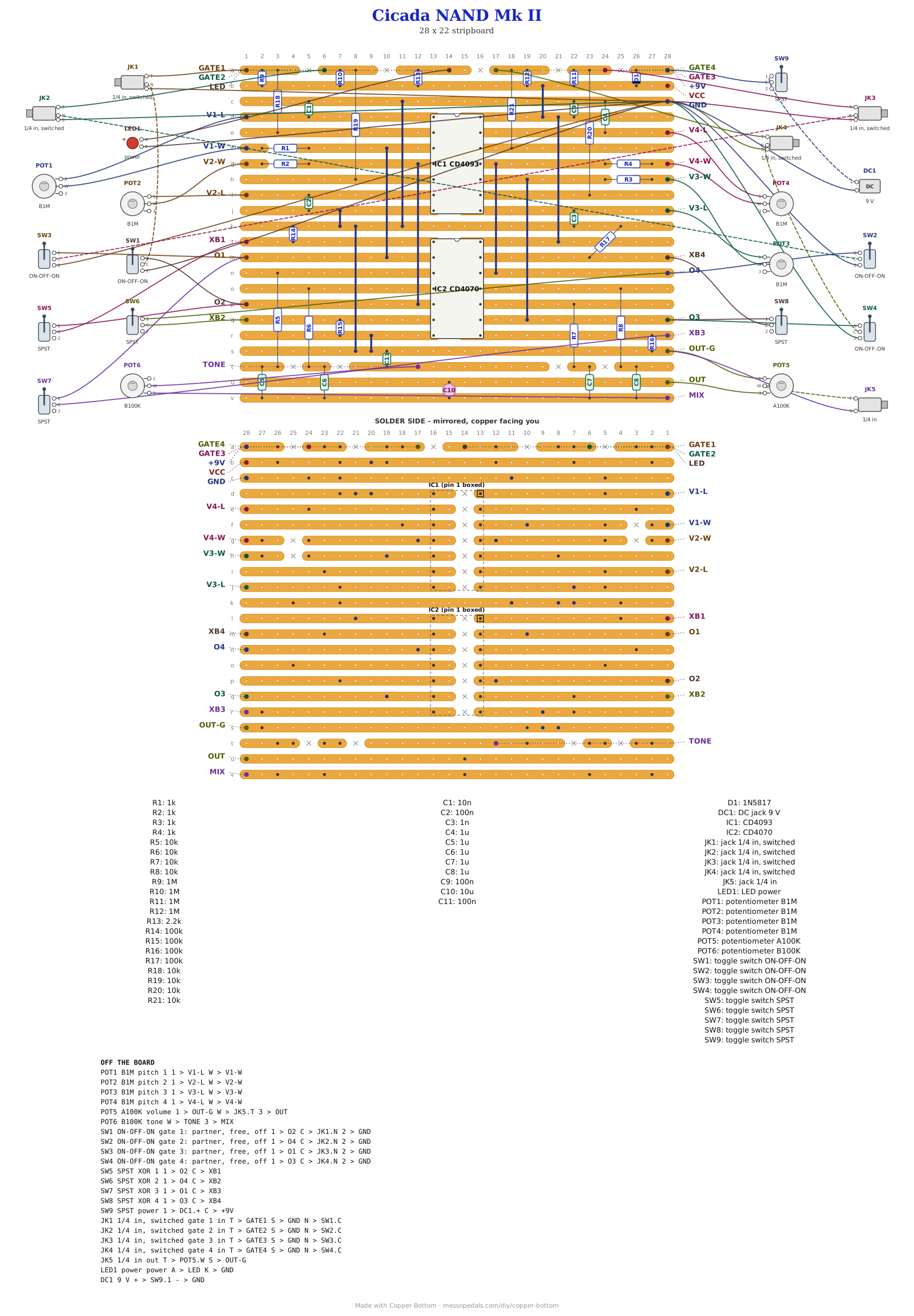
What you'll need
tap to expand / collapse
Thirty-three parts on the board plus the two chips and ten links, and twenty-three off it.
- 1× CD4093 quad Schmitt NAND, DIP-14 (IC1) - spot it: 4093 printed on top, a notch or a dot at the pin 1 end. The four voices. It is the upper chip
- 1× CD4070 quad XOR, DIP-14 (IC2) - spot it: 4070 printed on top. One XOR per voice, between the voice and the mix. It is the lower chip. Both solder straight to the board
- 4× 1K resistor (R1 to R4) - spot it: bands brown-black-red. One in series with each pitch pot, and not optional: at zero ohms the gate's output ties straight to its own input and the voice dies into a short
- 4× 10K resistor (R5 to R8) - spot it: bands brown-black-orange. The mixer, one per voice, the long ones running down to the bottom of the board
- 4× 10K resistor (R18 to R21) - the same bands. One from each gate pad down to its pin on IC1; it keeps whatever is plugged into a gate jack from pushing current straight into the chip
- 4× 1M resistor (R9 to R12) - spot it: bands brown-black-green. The gate pull-ups, standing on the top two strips. Each holds a gate high, so every voice plays with nothing connected
- 4× 100K resistor (R14 to R17) - spot it: bands brown-black-yellow. Each holds an XOR's second input low, so the voice passes straight through until its XOR toggle is closed
- 1× 2.2K resistor (R13) - spot it: bands red-red-red. For the power LED, which is off the board. It stands up near the top
- 4× ceramic timing caps - the ladder is the Mk I's: C1
103(10 nF), C2104(100 nF), C3102(1 nF) and C4105(1 µF). Each one sets that voice's register - 2× 100 nF ceramic (C9, C11) - spot it: printed
104. C9 sits across the supply beside IC1; C11 is the tone cap, near the bottom - 4× 1 µF film or other non-polarized cap (C5 to C8) - spot it: a small box printed
105. The mixer, one per voice. Each stands across two strips, to fit a 5 mm box - 1× 10 µF electrolytic (C10) - spot it: a small can with a stripe down one side; the stripe leg is the negative one. The output cap, stripe toward strip u, OUT
- 1× 1N5817 Schottky (D1) - spot it: black body, a gray band at one end. Reverse-polarity protection on the supply. It stands up on strips a and b, band on strip b
- 10× wire links - offcuts of component leg. All ten are straight and none runs under a chip
Off the board
- 4× B1M linear pots - pitch 1 to 4, two lugs each. Lug 1 to Vn-L, wiper to Vn-W. Lug 3 stays empty. A variable resistor, the same wiring as the Mk I
- 4× switched 1/4 inch jacks - the gate inputs. Tip to GATEn, sleeve to GND, and the switched lug, the one that touches the tip with nothing plugged in, to the middle lug of that voice's gate toggle
- 4× on-off-on toggles - the gate toggles. Middle lug to the jack's switched lug. One outer lug to the partner's O pad (see the table below), the other to GND. Center is free, one side is the partner, the other side is off
- 4× SPST toggles - the XOR toggles. One lug to XBn, the other to the partner's O pad
- 1× A100K log pot - volume. Lug 3 to OUT, lug 1 to OUT-G, wiper to the output jack tip
- 1× B100K linear pot - tone, two lugs. Lug 3 to MIX, wiper to TONE. Lug 1 stays empty
- 1× 1/4 inch jack - the output. Tip to the volume wiper, sleeve to OUT-G
- 1× LED - the power light. Long leg to LED, short leg to GND
- 1× DC jack, 9 V center negative
- An SPST toggle for power, in the positive supply lead between the DC jack and the board's +9V pad. Every build on this shelf gets one, and the drawing above shows it
- A box. Six knobs, nine toggles and seven jacks will not go on a 125B. A 1590BB is the smallest I would try, and there is no drill template for this one yet
The layout file is the guide
Like every layout on this shelf, the build document for this one is the file itself: ↓ Download Cicada_NAND_Mk_II.json - import it into Copper Bottom and the editor gives you the board picture, the placement walkthrough, the electrical checks and a printable build sheet, all from the same file. No coordinates are written out on this page on purpose: the editor is the viewer, and a number typed twice is a number that can drift.
Copper Bottom reports this one clean. The VCC pad is a test point for a meter, there so the checker knows that strip is the supply; nothing is wired to it.
The netlist
tap to expand / collapse
My script wrote this from the design and the board was checked against it in Copper Bottom: every connection it names is on the board and nothing on the board is missing from it. The same script checks that the four oscillators keep the Mk I's timing caps, 1Ks, mixer values and pull-ups. Each voice's nets start with its number: LUG and WIP are the pitch pot, OUT the voice itself, EN the NAND's gate input, GATE the jack and toggle side of it, XB the XOR's second input, X the XOR's output and M the point between its mixer resistor and cap. Voices 2 and 4 take their timing cap on the other input of their gate from the Mk I; a NAND does not care which.
The off-board wiring
Twenty-eight pads leave the board. VCC is only a test point.
| Pad | Goes to |
|---|---|
| V1-L … V4-L V1-W … V4-W | The four pitch pots: lug 1 to L, wiper to W, lug 3 empty. If one runs backwards, move its L wire to lug 3 |
| GATE1 … GATE4 | Each to its gate jack's tip. Bare, the voice plays |
| O1 … O4 | Each voice's own output, for the toggles of the voice it partners: one outer lug of that voice's gate toggle and one lug of its XOR toggle |
| XB1 … XB4 | Each to one lug of its XOR toggle. Bare, the voice passes straight through |
| OUT / OUT-G | Volume pot lug 3 and lug 1. The wiper goes to the output jack tip, and OUT-G to the jack sleeve as well |
| MIX / TONE | Tone pot lug 3 and wiper |
| LED | The power LED's long leg; its short leg to GND |
| +9V / GND | The supply, through the power toggle: DC jack positive to the toggle and the toggle to +9V, negative to GND. GND also takes the four gate jacks' sleeves and the four gate toggles' off lugs |
| VCC | Nothing. A test point: the supply after D1 |
The partners
Each voice has one partner, and both of its toggles reach for it. The order follows the timing caps, so each voice is chopped by the next one down in register, and the lowest voice is chopped by the highest.
| Voice | Its cap | Its partner | Its toggles go to |
|---|---|---|---|
| 1 | 10 nF | Voice 2 | O2 |
| 2 | 100 nF | Voice 4 | O4 |
| 3 | 1 nF, the highest | Voice 1 | O1 |
| 4 | 1 µF, the lowest | Voice 3 | O3 |
A plug in a gate jack takes over from that voice's gate toggle. The 4093 switches somewhere around half to two thirds of its supply, so a gate coming in wants about 7 V or more to be sure of opening a voice. Anything from my 9 V boxes is plenty. A 5 V Eurorack gate may not be.
Before you play
Turn the volume down, put every gate toggle in the middle and every XOR toggle open, and switch it on: the power LED should light. Then meter to ground. These numbers are the datasheets and arithmetic, not off a built board.
| Meter | Expect |
|---|---|
| The VCC pad, IC1 pin 14, IC2 pin 14 | The supply minus about 0.3 V, the drop across D1 |
| GATE1 to GATE4 | Nearly the full supply. Flip a gate toggle to off and its pad should read zero |
| XB1 to XB4 | Zero |
| O1 to O4 | About half the supply: a meter reads a running square that way. The slowest voice will swing the needle when its pitch knob is at the slow end |
If one voice is silent, meter its GATE pad first, then its O pad. A GATE pad at zero with the toggle in the middle points at that voice's jack: with nothing plugged in, its switched lug should touch the tip.
How it works, in one breath
Each voice is a Schmitt NAND with a cap from one input to ground and the pitch pot and its 1K from the output back to that input: the cap charges and drains across the gate's two thresholds and it oscillates. The NAND's other input is the gate. Held high, the voice runs; pulled low, it stops with its output stuck high, which the mixer caps hear as silence. The gate toggle's partner position puts another voice's square wave on that input, so the voice only sounds while its partner is high.
Every voice then goes through one XOR gate of IC2 on its way to the mix. With the second input held low by its 100K, an XOR passes the voice through unchanged. Close the XOR toggle and the second input is the partner, and the slot plays the two waves' XOR: high when they differ, low when they agree, which comes out as their sum and difference tones, the simplest ring modulator there is. After the four 10K and 1 µF pairs meet at MIX, the tone pot and C11 roll off the top, darkest at zero ohms, and the volume pot is a plain divider into the jack.
Things to try
None of these have been tried on this board.
- A photocell on a gate. Across a GATE pad and ground it is a light-gated voice, the trick the Mk I's page always offered
- The Spider into the gates. The Spider Sequencer runs on 9 V, so its steps can open the voices one at a time
- Gate and XOR on the same voice. Chopped by its partner and XORed with it at the same time. What that does depends on where the partner's knob is
The same circuit on a breadboard
tap to expand / collapse
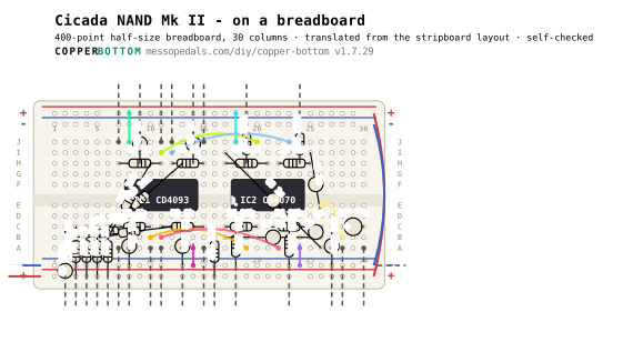
Want to hear it before you solder it? This is the layout file above moved onto a half-size breadboard, 30 columns by Copper Bottom's to breadboard button, in 76 steps with exact holes. It is a translation, not a copy: a strip and a breadboard column are different shapes, so every part is placed fresh and the stripboard's wire links are not needed.
Checked by the app, not built by me. Copper Bottom rebuilt the connections from these holes alone and compared them with the stripboard: all 122 terminals land on the same nets. Nobody has built this breadboard version.
Note. +9V is a second positive supply net. A breadboard rail carries one net, and the + rail here is VCC, so +9V rides ordinary columns - follow its steps, not the rail.
Turn the board so the numbers climb left to right. Then A to E is the lower bank, F to J the upper, the top rails are above J and the bottom rails below A.
The semiconductors
| Step | Do |
|---|---|
| 1 | Seat IC1 (CD4093) across the center channel, notch to the LEFT: pin 1 in E8, pin 14 in F8. Pins 1-7 run E8 to E14; pins 8-14 run back F14 to F8. Anywhere in the same bank and column is the same point - E8 and A8 are both pin 1. |
| 2 | Seat IC2 (CD4070) across the center channel, notch to the LEFT: pin 1 in E18, pin 14 in F18. Pins 1-7 run E18 to E24; pins 8-14 run back F24 to F18. Anywhere in the same bank and column is the same point - E18 and A18 are both pin 1. |
| 3 | Diode D1 (1N5817 Schottky): C2 to bottom + rail. The SECOND hole named gets the banded end - the cathode. Backwards, nothing works at all. |
Jumpers
| Step | Do |
|---|---|
| 4 | Jumper: J8 to the top + rail (IC1.14 to VCC). |
| 5 | Jumper: J18 to the top + rail (IC2.14 to VCC). |
| 6 | Jumper: A14 to the bottom − rail (IC1.7 to GND). |
| 7 | Jumper: A24 to the bottom − rail (IC2.7 to GND). |
| 8 | Jumper: B10 to A19 (@O1 to IC2.2). |
| 9 | Jumper: B11 to A22 (@O2 to IC2.5). |
| 10 | Jumper: I11 to J20 (IC1.11 to IC2.12). |
| 11 | Jumper: I12 to J23 (IC1.10 to IC2.9). |
| 12 | Jumper: E26 to B28 (C8.B to @MIX). |
| 13 | Jumper: tie the top + rail to the bottom + rail at the right-hand end, so they are one rail. |
| 14 | Jumper: tie the top − rail to the bottom − rail at the right-hand end, so they are one rail. |
Resistors
| Step | Do |
|---|---|
| 15 | Resistor R1 (1k): C10 to C7. |
| 16 | Resistor R2 (1k): C11 to C15. |
| 17 | Resistor R3 (1k): H12 to H15. |
| 18 | Resistor R4 (1k): H11 to H7. |
| 19 | Resistor R5 (10k): C20 to C17. |
| 20 | Resistor R6 (10k): C21 to C25. |
| 21 | Resistor R7 (10k): H22 to H25. |
| 22 | Resistor R8 (10k): H21 to H17. |
| 23 | Resistor R9 (1M): bottom + rail to C3. |
| 24 | Resistor R10 (1M): bottom + rail to C4. |
| 25 | Resistor R11 (1M): bottom + rail to C5. |
| 26 | Resistor R12 (1M): bottom + rail to C6. |
| 27 | Resistor R13 (2.2k): bottom + rail to C16. |
| 28 | Resistor R14 (100k): C18 to bottom − rail. |
| 29 | Resistor R15 (100k): C23 to bottom − rail. |
| 30 | Resistor R16 (100k): H24 to top − rail. |
| 31 | Resistor R17 (100k): H19 to top − rail. |
| 32 | Resistor R18 (10k): C9 to B3. |
| 33 | Resistor R19 (10k): C12 to B4. |
| 34 | Resistor R20 (10k): H13 to B5. |
| 35 | Resistor R21 (10k): H10 to B6. |
Ceramics and film
| Step | Do |
|---|---|
| 36 | Cap C1 (10n): C8 to bottom − rail. |
| 37 | Cap C2 (100n): C13 to bottom − rail. |
| 38 | Cap C3 (1n): H14 to top − rail. |
| 39 | Cap C4 (1u): H9 to top − rail. |
| 40 | Cap C5 (1u): B17 to B26. |
| 41 | Cap C6 (1u): B25 to C26. |
| 42 | Cap C7 (1u): I25 to D26. |
| 43 | Cap C8 (1u): I17 to A26. |
| 44 | Cap C9 (100n): bottom + rail to bottom − rail. |
| 45 | Cap C11 (100n): C27 to bottom − rail. |
Electrolytics
| Step | Do |
|---|---|
| 46 | Cap C10 (10u): + leg into C28, − leg into C30. The stripe on the can marks the MINUS leg. Backwards, an electrolytic eventually vents. |
Off-board
| Step | Do |
|---|---|
| 47 | Wire for +9V: into A2. This is where DC jack +, through the power switch joins the board. |
| 48 | Wire for GATE1: into A3. This is where gate 1 jack tip; the jack's switched lug goes to gate toggle 1's middle lug joins the board. |
| 49 | Wire for GATE2: into A4. This is where gate 2 jack tip; the jack's switched lug goes to gate toggle 2's middle lug joins the board. |
| 50 | Wire for GATE3: into A5. This is where gate 3 jack tip; the jack's switched lug goes to gate toggle 3's middle lug joins the board. |
| 51 | Wire for GATE4: into A6. This is where gate 4 jack tip; the jack's switched lug goes to gate toggle 4's middle lug joins the board. |
| 52 | Wire for LED: into A16. This is where power LED long leg (anode) joins the board. |
| 53 | Wire for MIX: into A28. This is where tone pot lug 3 joins the board. |
| 54 | Wire for O1: into A10. This is where voice 1 out, for the toggles that follow it: gate toggle 3's up lug and XOR toggle 3 joins the board. |
| 55 | Wire for O2: into A11. This is where voice 2 out, for the toggles that follow it: gate toggle 1's up lug and XOR toggle 1 joins the board. |
| 56 | Wire for O3: into J12. This is where voice 3 out, for the toggles that follow it: gate toggle 4's up lug and XOR toggle 4 joins the board. |
| 57 | Wire for O4: into J11. This is where voice 4 out, for the toggles that follow it: gate toggle 2's up lug and XOR toggle 2 joins the board. |
| 58 | Wire for OUT: into A30. This is where volume pot lug 3 joins the board. |
| 59 | Wire for TONE: into A27. This is where tone pot wiper (lug 1 left empty) joins the board. |
| 60 | Wire for V1-L: into A8. This is where pitch 1 pot lug 1 joins the board. |
| 61 | Wire for V1-W: into A7. This is where pitch 1 pot wiper (lug 3 left empty) joins the board. |
| 62 | Wire for V2-L: into A13. This is where pitch 2 pot lug 1 joins the board. |
| 63 | Wire for V2-W: into A15. This is where pitch 2 pot wiper (lug 3 left empty) joins the board. |
| 64 | Wire for V3-L: into J14. This is where pitch 3 pot lug 1 joins the board. |
| 65 | Wire for V3-W: into J15. This is where pitch 3 pot wiper (lug 3 left empty) joins the board. |
| 66 | Wire for V4-L: into J9. This is where pitch 4 pot lug 1 joins the board. |
| 67 | Wire for V4-W: into J7. This is where pitch 4 pot wiper (lug 3 left empty) joins the board. |
| 68 | Wire for XB1: into A18. This is where XOR toggle 1, one lug; its other lug goes to O2 joins the board. |
| 69 | Wire for XB2: into A23. This is where XOR toggle 2, one lug; its other lug goes to O4 joins the board. |
| 70 | Wire for XB3: into J24. This is where XOR toggle 3, one lug; its other lug goes to O1 joins the board. |
| 71 | Wire for XB4: into J19. This is where XOR toggle 4, one lug; its other lug goes to O3 joins the board. |
| 72 | Wire for OUT-G: into the bottom − rail. This is where volume pot lug 1 and the output jack sleeve joins the board. |
Power up
| Step | Do |
|---|---|
| 73 | GND - DC jack - (center pin, 9V center-negative), the power LED's short leg, the four gate jacks' sleeves and the four gate toggles' down lugs: clip to the bottom − rail. |
| 74 | VCC - test point: the supply after D1, about 8.7V on a 9V supply; nothing is wired here: clip to the bottom + rail. |
| 75 | Before the battery: meter on continuity. rail to rail reads open, not a short J8 to top + rail beeps (IC1.14 to VCC) J18 to top + rail beeps (IC2.14 to VCC) A14 to bottom − rail beeps (IC1.7 to GND) A24 to bottom − rail beeps (IC2.7 to GND) B10 to A19 beeps (@O1 to IC2.2) B11 to A22 beeps (@O2 to IC2.5) I11 to J20 beeps (IC1.11 to IC2.12) I12 to J23 beeps (IC1.10 to IC2.9) |
| 76 | Power on. |
Translated by Copper Bottom v1.7.29 from Cicada_NAND_Mk_II.json.
Circuit after the classic 4093 oscillator bank, the same idea as the Cicada NAND and the Dead-Bug Cicada; the XOR mix is out of every CMOS cookbook. The layout and the words are mine, and so is anything wrong with them.