Mantis
Eight-step up/down sequencer · By Onion Madder · Mess O' Pedals
An eight-step sequencer that runs forward or backward. Eight knobs each set one step, a clock walks through them, and one toggle decides which way it walks. It does not make a sound of its own: it makes a stepped voltage, a CV, for the pitch input of another build, so a VCO with a CV jack plays a little eight-note pattern that you can flip into reverse.
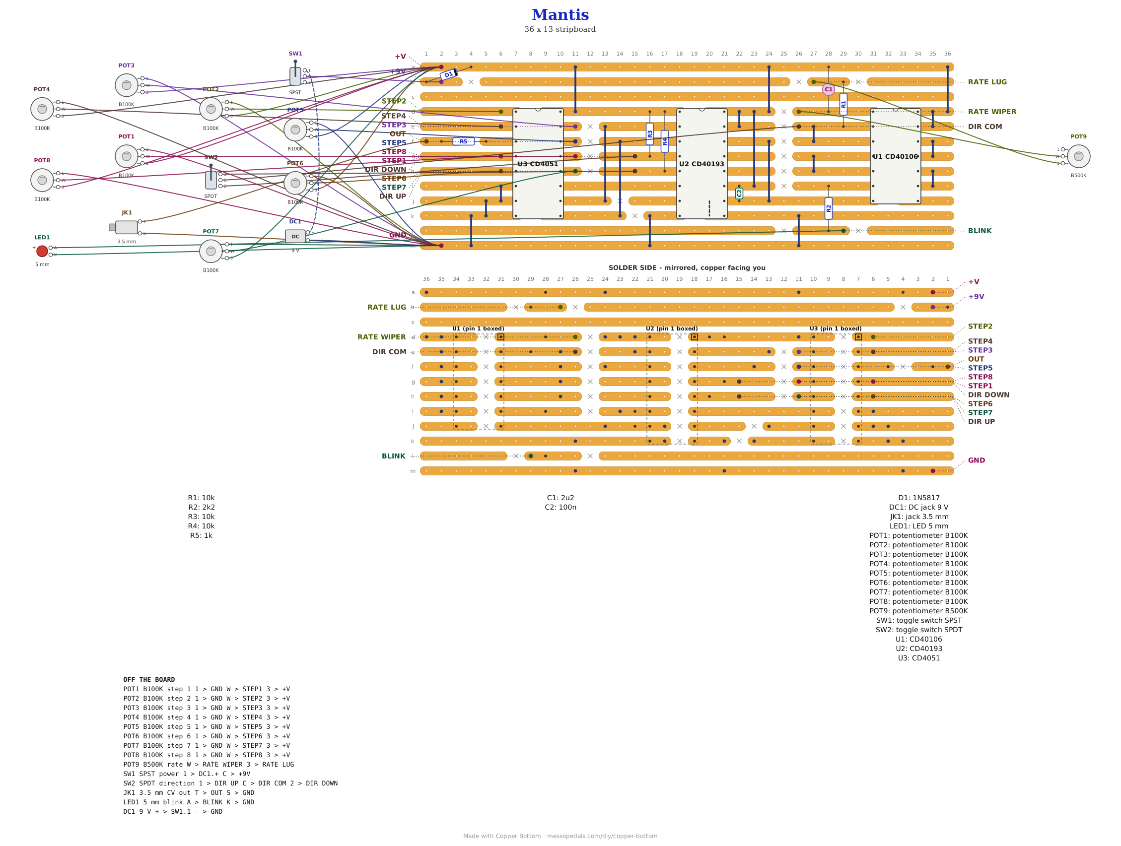
What you'll need
tap to expand / collapse
Three chips, eight small parts and 19 links on the board, and a box full of knobs off it. Every chip solders straight to the board.
- 1× CD40106 hex Schmitt inverter, DIP-14 (U1) - spot it: fourteen legs, CD40106 or HEF40106 on top. It is the clock
- 1× CD40193 up/down counter, DIP-16 (U2) - spot it: sixteen legs, CD40193 on top. Not a CD40192: that one counts to ten and would never reach some of the steps
- 1× CD4051 eight-channel switch, DIP-16 (U3) - spot it: sixteen legs, CD4051 or HEF4051 on top
- 3× 10K resistor (R1, R3, R4) - spot it: brown-black-orange. R1 is in series with the RATE pot; R3 and R4 hold the counter's two clock inputs high
- 1× 2.2K resistor (R2) - spot it: red-red-red. It feeds the blink LED
- 1× 1K resistor (R5) - spot it: brown-black-red. It lies along strip f over a cut, in front of the output
- 1× 2.2 µF electrolytic (C1) - spot it: a small can with a stripe down one side marking the negative leg; the file shows which way it goes. It sets the clock's range
- 1× 100nF ceramic (C2) - spot it: printed 104. The counter's supply bypass
- 1× 1N5817 Schottky (D1) - spot it: fat black body, gray band. It stops a supply plugged in backwards
- 19× wire links - offcuts of component leg. One, J11, runs under U2's body; that is ordinary
Off the board
- 8× B100K linear pots - STEP 1 to STEP 8. Each one's lug 3 goes to +V and lug 1 to GND, daisy-chained from pot to pot, and its wiper to its own STEP pad
- 1× B500K linear pot - RATE, wiper and one outer lug
- 1× SPDT toggle - DIR, forward or backward
- An SPST toggle for power, in the supply's plus lead before the board's +9V pad. Every build on this shelf gets one, and the drawing above shows it
- 1× 5 mm LED - it blinks with the clock
- 1× 3.5 mm jack - the CV out
- 1× 2.1 mm DC jack for a 9 V center-negative pedal supply
- A box with room for nine knobs, two toggles, an LED and two jacks. Nobody has drawn a drill template for this one yet
The layout file is the guide
Like every layout on this shelf, the build document is the file: ↓ Download Mantis.json - import it into Copper Bottom and the editor gives you the board picture, the placement walkthrough, the electrical checks and a printable build sheet, all from the same file. No coordinates are written out on this page on purpose: the editor is the viewer, and a number typed twice is a number that can drift.
Strip a is +V and strip m is ground. R5 lies along strip f over a cut, so its two legs are on different copper even though they share a strip. The chips go in last: solder everything else, do the meter check below, then the chips.
The steps play in order
The counter's three outputs drive the 4051's three select pins, but not in the order you would guess: Q3 drives A, Q2 drives B and Q1 drives C, because that is the wiring that fits the board. So as the counter counts, the 4051 reads its channels as 0, 4, 2, 6, 1, 5, 3, 7. That does not matter to you, because the STEP pads are numbered in the order they play: STEP 1 plays first and STEP 8 last going forward, and the other way around when DIR is flipped.
The netlist
My script wrote this from the design and checked the board against it, and so did Copper Bottom: every connection the netlist names is on the board and nothing on the board is missing from it. Four chip outputs are left empty on purpose, so the netlist does not mention them: U2 pins 7, 12 and 13 (Q4, CARRY and BORROW) and U1 pin 8.
The off-board wiring
| Pad | Goes to |
|---|---|
| +9V | DC jack +, through the power switch |
| GND | DC jack -, the output jack sleeve, the blink LED's cathode, and lug 1 of all eight step pots |
| +V | lug 3 of all eight step pots, daisy-chained |
| OUT | output jack tip: the stepped CV, into another build's CV or pitch input |
| DIR COM | DIR toggle (SPDT) middle lug: the clock |
| DIR UP | DIR toggle (SPDT) one end lug |
| DIR DOWN | DIR toggle (SPDT) other end lug |
| RATE WIPER | RATE pot wiper (lug 2) |
| RATE LUG | RATE pot lug 3 (lug 1 empty) |
| BLINK | blink LED anode (long leg); its cathode to GND |
| STEP1 | step pot 1 wiper |
| STEP2 | step pot 2 wiper |
| STEP3 | step pot 3 wiper |
| STEP4 | step pot 4 wiper |
| STEP5 | step pot 5 wiper |
| STEP6 | step pot 6 wiper |
| STEP7 | step pot 7 wiper |
| STEP8 | step pot 8 wiper |
First power-up
- Before the chips go in. Plug in the 9 V supply, switch on, and check for about 8.7 V from the GND pad to strip a, and to the holes where the three chips' supply pins go: U1 pin 14, U2 pin 16 and U3 pin 16
- Switch off, solder the three chips in, notch the way the file shows, and switch on. The blink LED should flash with the clock, and RATE should speed it up and slow it down
- Set the eight step pots to different places and put a meter on OUT. With RATE slow, the reading should step from one pot's setting to the next, and flipping DIR should send it back the other way
- Then plug OUT into the CV input of a VCO: the Mosquito 556 and the Opto Duet CV both have one
How it works, in one breath
One Schmitt inverter of the CD40106, with R1 and the RATE pot from its output back to its input and C1 on the input, is the clock: from about one step a second to about fifty, by arithmetic. Two more inverters copy it to light the LED. The DIR toggle sends the clock to one of the CD40193's two clock inputs, CLOCK UP or CLOCK DOWN, and R3 and R4 hold whichever one is not chosen high, which the counter needs before it will count on the other. Its outputs, three bits, choose which of the CD4051's eight channels is joined to its COM pin, and each channel is a pot's wiper sitting somewhere between 0 and +V. COM goes out through R5 as the CV.
Things to try
None of these have been tried, because none of this has.
- Slower. C1 at 10 µF stretches the clock about four and a half times, into a slow walk
- A photocell for RATE, across RATE WIPER and RATE LUG, and the pattern speeds up in the light
- Into the Mosquito 556's CV jack, with its pitch knob setting where the pattern sits
A counter stepping a 4051 through a row of pots is the standard analog sequencer, and belongs to everyone who has built one. This up/down version and its layout were drawn for this site, and anything wrong with them is mine to fix.