AD/AR Envelope
One supply, one chip, two knobs · By Onion Madder · Mess O' Pedals
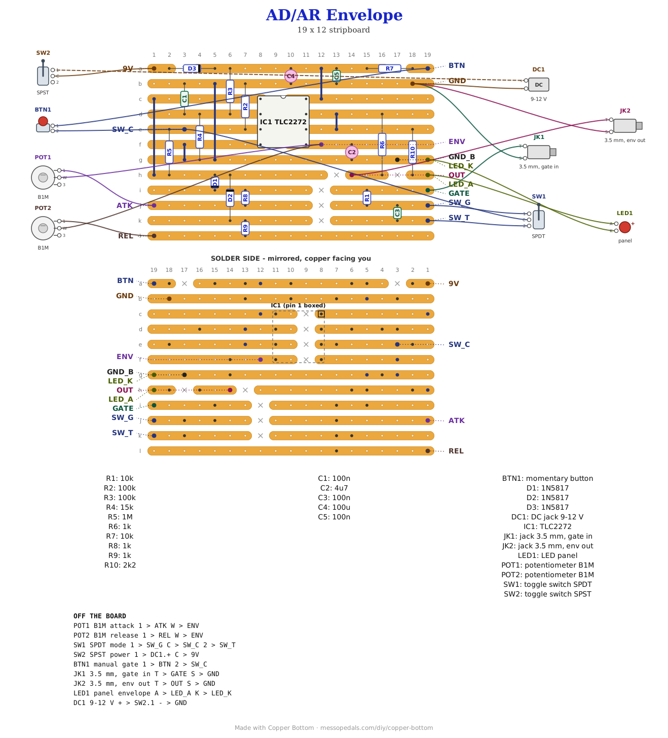
An envelope generator turns a gate into a shape: press a key, or send a pulse, and it puts out a voltage that climbs, holds or falls, and dies away. Point that at a VCA or a filter and a drone becomes notes. This is Sam Battle's simple AD/AR from LookMumNoComputer, by way of Eddy Bergman's stripboard layout of it, redrawn to run from one 9 to 12 V supply instead of a ±12 V rack. Two knobs, attack and release. A toggle picks AR, where the envelope holds for as long as the gate does, or AD, where only the rising edge counts. A button fires it by hand, and an LED shows you the shape.
What you'll need
tap to expand / collapse
Twenty-three parts on the board, counting the links, and nine off it. The op-amp is the one part to buy carefully.
- 1× TLC2272 or TLV2372 dual op-amp, DIP-8 (IC1) - spot it: eight legs, the number printed on top, a notch at one end. It has to be rail-to-rail on the output, because the envelope is the op-amp's output and a chip that stops short of the supply stops the envelope short too. An LM358 fits the socket and works, but tops out about 1.5 V under the supply, and its input current droops a long release. A TL072 will not do on one supply. Fit a socket
- 3× 1N5817 Schottky (D1, D2, D3) - spot it: fat black body, a gray band at one end. D1 and D2 steer the charge one way through the attack knob and the other way through the release knob; D3 stops a backwards plug
- 1× 1M resistor (R5) - spot it: bands brown-black-green. A little positive feedback, so a slow gate edge snaps cleanly
- 2× 100K resistor (R2, R3) - spot it: bands brown-black-yellow. R2 holds the gate at zero when nothing is plugged in; R3 is the top of the reference divider
- 1× 15K resistor (R4) - spot it: bands brown-green-orange. The bottom of the divider: the gate has to clear about 1.2 V on a 9 V supply, 1.6 V on 12
- 2× 10K resistor (R1, R7) - spot it: bands brown-black-orange. R1 protects the gate input; R7 feeds the manual button
- 1× 2K2 resistor (R10) - spot it: bands red-red-red. The LED's series resistor
- 3× 1K resistor (R6, R8, R9) - spot it: bands brown-black-red. R6 protects the output from a shorted cable. R8 and R9 are the floors under the two knobs, so neither pot can reach zero ohms
- 1× 4.7 µF electrolytic (C2) - spot it: a small can with a stripe down one side. This is the timing cap, and the part to change for a longer or shorter range. Stripe to ground
- 1× 100 µF electrolytic (C4) - the supply reservoir. Stripe to ground
- 3× 100nF ceramic (C1, C3, C5) - spot it: printed 104. C1 keeps the reference quiet, C5 decouples the chip, and C3 turns a gate into a short trigger pulse in AD mode
- 5× wire links (J1 to J5) - offcuts of component leg
- 1× DIP-8 socket
Off the board
- 2× B1M linear pot - attack and release. Each is wired as a variable resistor: lug 1 to its pad (ATK or REL), the wiper to ENV, and the third lug left empty. Both wipers share the ENV pad. The 1K floor resistor each one needs is already on the board
- 1× SPDT toggle - the mode switch, AR or AD. Common to SW_C, the two outer lugs to SW_G and SW_T
- 1× momentary push button, normally open - the manual gate. One lug to BTN, the other to SW_C beside the toggle's common
- 2× 3.5 mm jacks - gate in and envelope out. Sleeves to GND
- 1× LED - long leg to LED_A, short leg to LED_K. R10 is on the board, so nothing else goes with it
- 1× DC jack, 9 to 12 V, center negative. D3 means a backwards plug does nothing
- An SPST toggle for power, in the positive supply lead between the DC jack and the board's 9V pad. Not in the layout file - it is off the board, and every build on this shelf gets one
The layout file is the guide
Like every layout on this shelf, the build document for this one is the file itself: ↓ Download AD_AR_Envelope.json - import it into Copper Bottom and the editor gives you the board picture, the placement walkthrough, the electrical checks and a printable build sheet, all from the same file. No coordinates are written out on this page on purpose: the editor is the viewer, and a number typed twice is a number that can drift.
Two ground strips, one net. Strips b and g both carry ground, one above the chip and one below it, joined by J2. That is what lets every capacitor span a single strip instead of five, which matters for the electrolytics: a radial can does not stretch half an inch without looking it. The columns under the chip carry nothing but the cut.
The netlist
Quoted verbatim from the layout file, and emitted from the copper rather than typed
beside it - so checking the board against it can only pass. What it is for is carrying the
circuit somewhere else, and telling you what each strip is doing while you stare at it. The
two lines worth finding are ATK_W and REL_W: each is a pad and one
resistor leg, and the knob goes between it and ENV.
The off-board wiring
Fourteen pads leave the board: two knobs, a toggle, a button, two jacks, an LED and the supply.
| Pad | Goes to |
|---|---|
| ATK / REL / ENV | The two B1M pots. Attack: lug 1 to ATK, wiper to ENV. Release: lug 1 to REL, wiper to ENV. Two wipers on one pad, third lugs empty. Variable resistors, not dividers - see the Cicada NAND for the same shape |
| SW_C / SW_G / SW_T | The mode toggle. Common to SW_C; SW_G is AR, the gate as it is; SW_T is AD, the gate through C3 so only its edge gets through |
| BTN | One lug of the manual button. The other lug goes to SW_C, so the button works in either mode |
| GATE | Gate in jack, tip. The sleeve goes to GND |
| OUT | Envelope out jack, tip. The sleeve goes to GND |
| LED_A / LED_K | The LED, long leg to LED_A. It follows the envelope |
| 9V / GND | The supply, through the power toggle. DC jack positive to the toggle and the toggle to 9V; negative to GND, which is also both jack sleeves. GND_B is a second ground pad on the same net, there if a wire is easier to land on that side |
How it works, in one breath
One half of the TLC2272 is a comparator. Its minus input sits on a small fixed reference from R3 and R4; its plus input is the gate. When the gate goes high the output snaps to the supply, and it pushes current through D1, R8 and the attack pot into C2, so C2 charges: that is the attack. When the gate goes low the output drops to ground and C2 drains the other way, through the release pot, R9 and D2: that is the release. The diodes are what keep the two knobs apart, one for each direction. The other half of the chip is a follower that copies C2 to the out jack without taking anything from it, and the LED hangs off the follower too.
The mode toggle decides what the comparator sees. In AR it sees the gate itself, so the envelope climbs and then holds at the top until you let go. In AD the gate goes through C3 first, which passes the rising edge and nothing after it: a pulse of about 10 ms from C3 against R2. That means in AD the comparator is only high for those 10 ms, so the attack knob shapes the very start and the release does the rest. That is how this circuit behaves, and it is a read of the circuit, not of a build.
Why one supply. The original runs on ±12 V with a TL072, so the comparator swings to −12 V and drags C2 down with it, and a diode on the output throws away everything below zero. On a long attack the cap has to climb back from −12 V before anything comes out, which builders report as the envelope starting late. Here C2 swings from 0 to the supply: there is no negative stretch to wait out, the output diode is gone, and the timing cap is an ordinary electrolytic instead of a bipolar one.
The arithmetic, and it is arithmetic and not a measurement. With C2 at 4.7 µF and a pot wide open at 1M, one time constant is about 4.7 seconds, so a full attack or release takes several seconds. At the bottom of the knob only the 1K floor is left, about 5 ms. The envelope tops out a Schottky drop, a few tenths of a volt, under the supply.
Things to try
None of these have been tried, because none of this has. They are the obvious knobs.
- Change C2. It sets the whole range. 10 µF doubles every time, 1 µF makes it snappy and percussive.
- Swap the pots. A B500K halves the longest time and gives the short settings, where most of the playable ones live, more of the knob.
- Leave the LED off. It is on the output side of the follower and does nothing for the envelope; if the box is dark on purpose, it can go.
- Drive it from the Spider Sequencer clock and put the out into a VCA, and each step gets its own swell.
The circuit is Sam Battle's, the simple AD/AR from LookMumNoComputer. The stripboard layout this one is derived from is Eddy Bergman's, Synthesizer Build part 14 at eddybergman.com, along with the changes Sam suggested to it and the builders' reports that the one-supply note above is built on. This board is not his hole for hole: it runs from one supply on a rail-to-rail op-amp, the output diode is gone, the timing cap is a polarized 4.7 µF, it adds decoupling, a reverse-polarity diode, a manual button and an envelope LED, and it is 228 holes where his is 528. Those are mine and so is anything wrong with them.