Paper Mosquito
The NE556 Atari Punk Console as a paper circuit · By Onion Madder · Mess O' Pedals
A paper circuit is a circuit board you print. The drawing is the board, the holes are poked with tweezers, and the traces are bare wire laid along the lines on the back. This one is the Dead-Bug Mosquito rebuilt on paper: one chip, ten parts, and it drones the moment it powers up. Same circuit, and the same values apart from the pitch pot, so if you have built that one, every connection here will look familiar.
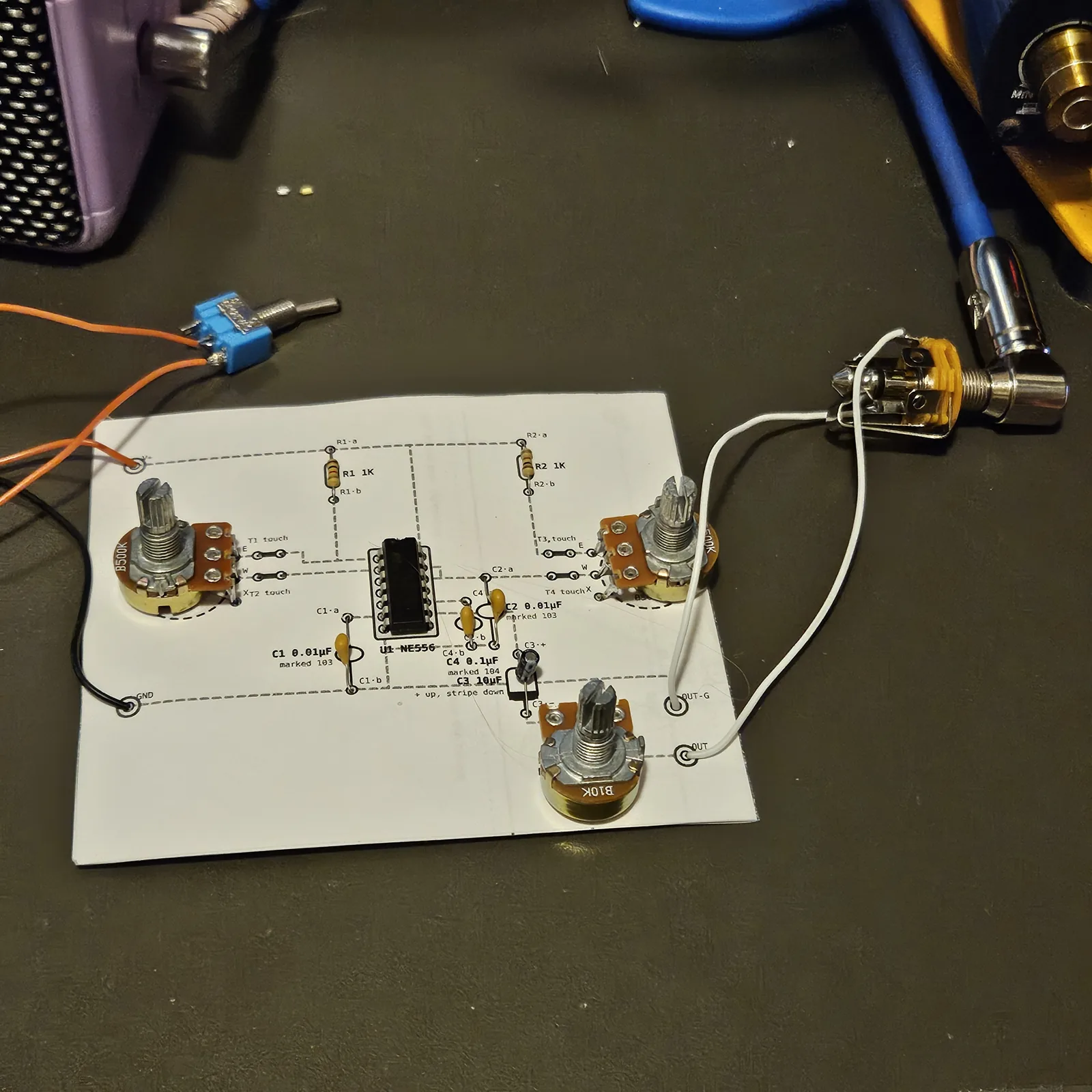
Why a paper series
I love the concept of Peter Blasser's paper circuits (Ciat-Lonbarde), but his are complicated, they use esoteric parts, and they are difficult to troubleshoot. If a beginner wants to try paper circuits, I think it can be made more accessible. That is the idea behind this series: circuits you already know, common parts, a sheet that tells you where everything goes, and a recipe you can check step by step.
⚠ Before you start tap to expand / collapse
Paper burns. Keep the iron moving, quick joints, and don't rest it on the sheet. Work over something that isn't flammable, and keep a damp sponge handy.
Socket the chip. Soldering straight to the NE556 means holding heat on paper right next to 14 tightly packed holes. The socket takes the heat instead, and the chip goes in last.
Bare traces on the back can short. The only place they run close is trace G under the socket, so keep it centered between the two rows of pins.
Loud and shrill. It's still an APC. Start with VOLUME low.
What you'll need
tap to expand / collapse
New to the parts? Each line notes how to spot it - the printed marking, the package, or the polarity clue.
- 1× NE556 dual timer and a 14-pin DIP socket - spot it: NE556 printed on top; a notch or dot marks pin 1. The socket is what saves the paper from chip-pin heat.
- 2× B500K pots (pitch and shape) - spot it: marked B500K; B = linear taper, and the middle lug is the wiper. I used B500K for both. The sheet prints B1M for pitch, which is what the Dead-Bug Mosquito uses, and a B1M works in either spot, just with a wider range.
- 1× B10K pot (volume) - spot it: marked B10K (B5K is fine)
- 2× 1K resistors (R1, R2) - spot it: bands brown-black-red; non-polar
- 2× 0.01 µF ceramic (C1, C2) - spot it: tiny disc printed 103
- 1× 0.1 µF ceramic (C4) - spot it: disc printed 104
- 1× 10 µF electrolytic (C3) - spot it: a little can; the stripe marks the minus leg, and the long leg is plus
- Bare tinned wire - for the traces on the back
- Insulated wire, white and yellow - J1 and J2 are white, J3 is yellow
- An SPST toggle, a jack or an 8 Ω speaker, and a power source: at least two vape cells in series (7.4V; three gives 11.1V), or a 9V battery
- Cereal-box card cut to 110 × 95 mm, a glue stick, and sharp tweezers - the tweezers poke the holes
Quick reference - the chip and the traces
Parts go in from the printed front, so the socket on the front reads exactly like this map. On the back it's mirrored, which is why the back half of the sheet prints pin numbers next to every hole.
Around the socket
- J1, white: pin 4 → pin 14
- J2, white: pin 10 → pin 14
- J3, yellow: pin 5 → pin 8
- N: pin 13 → pin 12
- G: pin 2 → pin 6, down the middle of the socket
Timer A, the pitch
- E and D: R1·b → pin 1, with PITCH E on D
- F: PITCH W → pin 2
- H: C1·a → pin 6
Timer B, the shape
- P: SHAPE E → R2·b
- O: SHAPE W → C2·a → pin 12
- C: C4·a → pin 10
- K: C4·b and C2·b → J
Buses and output
- A, V+ bus: V+ → R1·a → R2·a, with B from pin 14
- I, ground bus: GND → C1·b, with J from pin 7, L and M
- Q: pin 9 → C3·+; R: C3·− → VOLUME IN
- S: VOLUME W → OUT
Reading the sheet
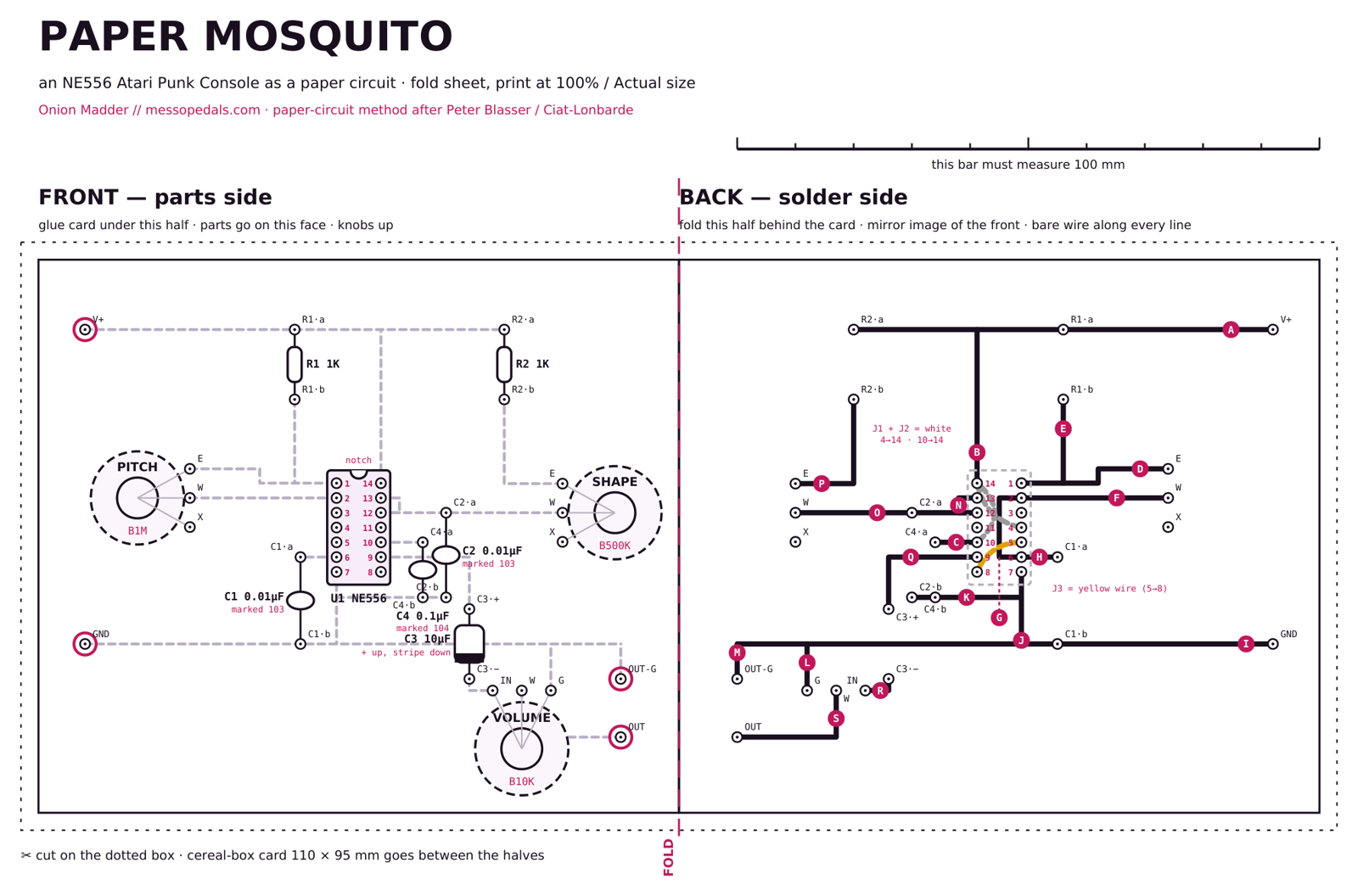
Front: each part is drawn where it sits, with its value printed next to it. The faint dashed lines are only a preview of what connects on the back, so you can see where a part goes without flipping the board. The four ringed holes (V+, GND, OUT, OUT-G) are for wires going off the board. Each pot has three holes: E (an end lug), W (the wiper, its middle lug) and X (the other end, left empty).
Back: every bold black line is a trace you make with bare wire or a bent part leg, tagged with a pink letter so the steps can name it. The dashed gray and yellow arcs are the three insulated wires. Small pink numbers beside the socket holes are the chip's pin numbers.
Steps 1–8 Print, fold, poke
The sheet is the circuit board. Print it, sandwich a piece of cereal-box card between the two halves, and poke every dot through all three layers. The back half is a mirror image of the front, so once it's folded the holes line up on both faces.
Print at 100% / “Actual size”. Fit-to-page shrinks it and the socket holes stop matching the chip.
| Step | Do |
|---|---|
| 1 | Print page 1 of the build sheet on plain printer paper at 100% / Actual size. |
| 2 | Measure the 100 mm bar at the top right of the sheet. If it isn't 100 mm, fix the print scale and print again. |
| 3 | Cut out the whole strip along the dotted box, both halves in one piece. |
| 4 | Cut a piece of cereal-box card exactly 110 × 95 mm. |
| 5 | Glue the card to the back of the FRONT half, edges lined up with the solid box. |
| 6 | Fold the BACK half over along the FOLD line and glue it to the other side of the card. |
| 7 | Poke the 14 U1 holes from the front with sharp tweezers, straight down through all three layers. |
| 8 | Poke the other 25 dots the same way. Check the back and open any hole that didn't come all the way through. |
Steps 9–16 Start in the middle: the socket
Everything builds outward from the chip. Each part goes in from the printed front, then on the back you bend its legs along its trace to the socket pin it belongs to and solder it there. Every part you add is anchored to the middle, so the whole thing gets stiffer as you go instead of floppier.
Quick dabs only. Paper scorches if you sit on it: touch, flow, lift.
| Step | Do |
|---|---|
| 9 | Push the 14-pin socket into the U1 holes from the front, notch toward the top edge (the drawn notch). |
| 10 | On the back, bend socket pins 1, 7, 8 and 14 outward slightly so the socket can't fall out. |
| 11 | Insulated white wire J1 from socket pin 4 to socket pin 14. Solder at pin 4 only. |
| 12 | Insulated white wire J2 from socket pin 10 to socket pin 14. Solder both wires at pin 14 together, then J2 at pin 10. |
| 13 | Insulated yellow wire J3 from socket pin 5 to socket pin 8. Solder at both pins. |
| 14 | Trace N: short bare wire from socket pin 13 to pin 12. Solder at both pins. |
| 15 | Trace G: bare wire from socket pin 2 down the middle of the socket to pin 6, centered between the two rows of pins. Solder at pin 2 and pin 6. |
| 16 | Trace J: bare wire from socket pin 7 down to the ground-bus line. Solder at pin 7 only; the far end gets soldered with the bus. |
Steps 17–25 Next ring out: the caps
The three small caps sit right beside the chip. Each one goes in from the front, and on the back one leg bends along its trace to a socket pin.
Leave the legs long until each one is soldered, then snip the tail.
| Step | Do |
|---|---|
| 17 | C4, 0.1 µF (marked 104): legs into C4·a and C4·b from the front. |
| 18 | On the back, bend C4·a's leg along trace C to socket pin 10. Solder at C4·a and at pin 10. |
| 19 | Bend C4·b's leg along trace K until it crosses trace J. Solder at C4·b and where it touches J. |
| 20 | C2, 0.01 µF (marked 103): legs into C2·a and C2·b from the front. |
| 21 | On the back, bend C2·a's leg along trace O to socket pin 12. Solder at C2·a and at pin 12. |
| 22 | Bend C2·b's leg along trace K to C4·b. Solder at C2·b and at C4·b. |
| 23 | C1, 0.01 µF (marked 103): legs into C1·a and C1·b from the front. |
| 24 | On the back, bend C1·a's leg along trace H to socket pin 6. Solder at C1·a and at pin 6. |
| 25 | Solder C1·b's leg in its hole and leave the tail long. The ground bus lands on it later. |
Steps 26–32 Out to the resistors and the output cap
Same move, one ring further out. The resistor legs are long enough to reach their traces on their own.
| Step | Do |
|---|---|
| 26 | R1, 1K (brown-black-red): legs into R1·a and R1·b from the front. |
| 27 | On the back, bend R1·b's leg down trace E, then along trace D to socket pin 1. Solder at R1·b and at pin 1. |
| 28 | R2, 1K: legs into R2·a and R2·b from the front. |
| 29 | On the back, bend R2·b's leg down trace P to its corner. Solder at R2·b only; the shape pot joins it later. |
| 30 | C3, 10 µF electrolytic: long + leg into C3·+, striped leg into C3·−, from the front. Lay the can flat over its drawing. |
| 31 | Trace Q: bare wire from socket pin 9 along the line to C3·+. Solder at pin 9 and at C3·+. |
| 32 | Bend C3·−'s leg along trace R so its end sits over the VOLUME IN hole. Solder at C3·− only. |
Steps 33–35 The two buses
Power along the top edge, ground along the bottom. Each one is a single straight bare wire, soldered wherever a part or trace meets it.
| Step | Do |
|---|---|
| 33 | Trace B: bare wire from socket pin 14 straight up to the V+ bus line. Solder at pin 14. |
| 34 | Trace A, V+ bus: bare wire from the V+ hole through R1·a to R2·a. Solder at V+, at R1·a, where it meets trace B, and at R2·a. |
| 35 | Trace I, ground bus: bare wire from the GND hole along the bottom line to the far end. Solder at GND, at C1·b, and where it meets trace J. |
Steps 36–47 The pots, outermost
The pots go in last because they're the heaviest. Push each pot's lugs through from the front, shaft up, middle lug (the wiper) in W. With solder-lug pots, solder a short wire to each lug and push the wires through instead.
| Step | Do |
|---|---|
| 36 | PITCH pot, B500K (the sheet says B1M; either works): lugs into the PITCH holes E, W and X. |
| 37 | Trace F: bare wire from PITCH W to socket pin 2. Solder at W and at pin 2. |
| 38 | Trace D: bare wire from PITCH E along the line to where R1's leg runs. Solder at E and where it touches R1's leg. X stays empty. |
| 39 | SHAPE pot, B500K: lugs into the SHAPE holes E, W and X. |
| 40 | Trace O: bare wire from SHAPE W to C2·a. Solder at W and at C2·a. |
| 41 | Trace P: bare wire from SHAPE E to the corner of R2's leg. Solder at E and where it touches R2's leg. X stays empty. |
| 42 | VOLUME pot, B10K: lugs into the VOLUME holes IN, W and G. |
| 43 | Solder VOLUME IN, where C3·−'s leg is already sitting. |
| 44 | Trace L: bare wire from VOLUME G up to the ground bus. Solder at G and at the bus. |
| 45 | Trace S: bare wire from VOLUME W to the OUT hole. Solder at W and at OUT. |
| 46 | Trace M: bare wire from the OUT-G hole up to the ground bus. Solder at OUT-G and at the bus. |
| 47 | Snip every leg tail that sticks past its joint. |
PITCH and SHAPE are variable resistors: only E and W are used, and X stays empty. R1 and R2 are the 1K in series with each one, which is why a pot does nothing at one end of its travel. VOLUME is a divider and uses all three lugs.
Steps 48–52 Off the board
Power and output hang off the four ringed holes on flying leads, same as the dead-bug build. Solder each wire on the back.
| Step | Do |
|---|---|
| 48 | Battery red (+) to one lug of the SPST toggle. |
| 49 | Other toggle lug to the V+ hole. |
| 50 | Battery black (−) to the GND hole. |
| 51 | Jack tip (or speaker +) to the OUT hole. |
| 52 | Jack sleeve (or speaker −) to the OUT-G hole. |
Steps 53–57 Check, then chip
Meter it before the chip goes in. If the socket is happy, the chip will be too.
| Step | Do |
|---|---|
| 53 | Toggle on, socket empty. Meter the V+ hole to the GND hole: battery voltage. |
| 54 | Meter socket pin 14 to pin 7: battery voltage. |
| 55 | Meter pin 4 to pin 7, then pin 10 to pin 7: battery voltage both times. |
| 56 | Toggle off. Push the NE556 into the socket, notch toward the top. |
| 57 | Toggle on with VOLUME low. It should drone right away. Sweep PITCH, then SHAPE. |
| Meter between | Expect (socket empty, toggle on) |
|---|---|
| V+ hole → GND hole | battery voltage (9V, or 7.4V on two vape cells) |
| Socket pin 14 → pin 7 | battery voltage |
| Socket pin 4 → pin 7, pin 10 → pin 7 | battery voltage (the resets) |
| Socket pin 5 → pin 8, with the meter on continuity | beep (J3) |
⚠ If it won't sing
| Symptom | Check |
|---|---|
| Dead silent | J1 and J2: pins 4 and 10 must read battery voltage. Then J3, then pin 14 and pin 7. |
| Silent, chip warm | Two bare traces touching on the back, most likely trace G brushing a pin. Look under the socket with a light behind the card. |
| Faint, or only a tick | C3 the wrong way around (+ goes in C3·+), or C1/C2 not reaching ground through traces I/K. |
| Putt-putt motorboating | C4 not soldered at both ends, or a cold joint on trace C or K. |
| A pot does nothing at one end | Normal: that is the 1K stopping it at zero. Does nothing at all: lug in the wrong hole, or the wiper isn't in W. |
| Paper scorched or a hole tore | Glue a scrap of paper over the back, re-poke, carry on. It is paper. |
Built, and heard
It sounds crazy different from a standard Mosquito. I don't know if it's the paper or what, but it sounds so fuzzy and ethereal.
Things to try
- Body contacts: solder a bare-wire staple onto trace D and another onto trace F, a few millimeters apart on the front. A fingertip across them bridges the pitch pot, so you play pitch by touch (works best with PITCH turned toward its slow end). An LDR across the same two points makes it follow light.
- CV inputs: pins 3 and 11 are left open, like the Mosquito. A 100K from either into a jack gives you the CV inputs from the Mosquito page.
- One and a half: hang an NE555 one-shot off pin 5 for the “one and a half” mod. Draw its traces onto your sheet in pen first.
- Color the front in. Blasser's sheets are half schematic, half drawing, and nothing on the front side carries current.
The APC descends from Forrest M. Mims III's “Stepped Tone Generator.” The paper-circuit method is Peter Blasser's / Ciat-Lonbarde's. This layout and the words are my own.