Paper Opto Duet Mk II
The Opto Duet with CV, a gate and a speaker amp as a heart-shaped paper circuit · By Onion Madder · Mess O' Pedals
The Opto Duet with everything I wanted to add to it. Two 555s still play each other through light, with a CV jack on tempo and one on pitch. Now a RANGE knob takes the voice from a squeal down to slow blips, a second cell beside the engine's LED pulses the volume as well as the pitch, and two toggles choose what the LED drives. A tone knob, a volume knob, a line out and a speaker amp sit at the end.
⚠ Before you start tap to expand / collapse
Paper burns. Keep the iron moving, quick joints, and don't rest it on the sheet. Work over something that isn't flammable, and keep a damp sponge handy.
Three chips, three ways. IC1 goes in notch down, IC2 notch up, IC3 notch left. All three solder straight to the paper with no socket, so check each notch against the drawing before the first joint.
Mind the cans. C1, C3, C6, C7, C11 and C12 are polarized: the stripe is the − leg, and the sheet marks each + hole.
10K is not 1K. R2 and R4 are brown-black-orange; the four 1Ks are brown-black-red. Swapped, the mix is wrong and the speaker amp gets far too much.
Parts bridge the lines. R4 lies across the middle ground line, and J1 to J3 cross bare wire on the back. Only part legs go through the paper, and J1 to J3 are insulated, so nothing touches what it crosses.
What you'll need
tap to expand / collapse
New to the parts? Each line notes how to spot it - the printed marking, the package, or the polarity clue.
- 2× NE555 (IC1, IC2) and 1× LM386 (IC3) - spot it: 8 pins each, the name printed on top, a notch or dot at pin 1. Any LM386 version. They solder straight to the paper, no socket.
- 4× LDR photocells (LDR1 to LDR4) - spot it: a little disc with a wavy track across its face; either way around. LDR1 is the tempo eye, LDR3 the pitch eye; LDR2 and LDR4 go in the sleeve with LED1.
- 3× LEDs (LED1, LED2, LED3) - spot it: long leg +. LED1 flashes into the cells, LED2 is the indicator, LED3 the power light.
- 1× 1N5817 Schottky diode (D1) - spot it: small black body; the band marks the cathode
- Resistors: 4× 1K, 2× 10K, 2× 4.7K, 2.2K, 220Ω, 10Ω - spot it: brown-black-red, brown-black-orange, yellow-violet-red, red-red-red, red-red-brown, brown-black-black
- Ceramic caps: 5× 0.1 µF, 2× 0.01 µF, 0.047 µF - spot it: little discs printed 104, 103 and 473
- Electrolytics: 2× 10 µF, 3× 100 µF, 220 µF - spot it: cans; the stripe marks the − leg
- 3× pots: B1M, B10K, A10K - spot it: RANGE, TONE and VOL. B is linear, A is log. On wires, so any style fits.
- 3× SPST toggles - spot it: power, PITCH and GATE, on wires
- 2× 3.5 mm jacks, a 1/4 in jack, a small 8Ω speaker - spot it: the two CV inputs, the line out, and the speaker, on wires
- Bare tinned wire, insulated wire, black heatshrink - spot it: bare for the traces, insulated for J1 to J3 and the wires off the board, heatshrink wide enough for LED1 and two cells
- A 9V battery and snap, or a 2.1 mm DC jack - spot it: for a center-negative 9V pedal supply
- Plain printer paper, a glue stick, scissors, pointed tweezers, a cardboard box - spot it: the core, the holes, and something to take the points
Quick reference - the chip
These are the chips the usual way up, notch at the top. On the sheet they sit three different ways: IC1 notch DOWN, IC2 notch UP, and IC3 on its side with the notch to the LEFT, so its pins 8, 7, 6, 5 run along the top row and 1, 2, 3, 4 along the bottom. Match each chip to its drawn notch. The sheet prints the number beside every chip hole on both faces. IC3's pins 1, 7 and 8 stay empty on purpose.
Reading the sheet
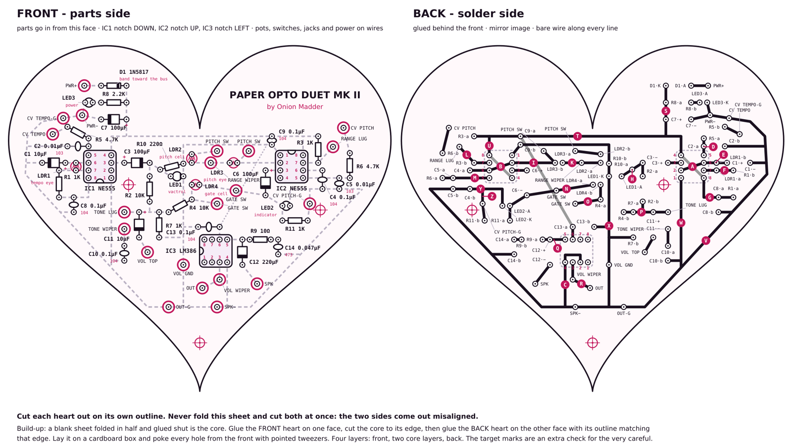
Front: each part is drawn where it sits, with its value printed next to it. The faint dashed lines are only a preview of what connects on the back. The ringed holes are for wires going off the board: PWR+ and PWR− for power; CV TEMPO, CV PITCH and their -G pads for the CV jacks; RANGE, TONE and VOL for the three pots; two PITCH SW and two GATE SW pads for the toggles; OUT and OUT-G for the line out; SPK and SPK− for the speaker. The three target marks are an extra check for the very careful: on the finished heart they sit on top of each other.
Back: every bold black line is bare wire or a bent part leg. The lines with a letter in a circle are bare wire, and the steps name them by that letter; the short unlettered ones are a part's own leg, bent along the line. Small pink numbers beside the chip holes are their pin numbers. The three wide gray lines are insulated wire, J1, J2 and J3: they cross bare lines, so they have to be insulated.
Steps 1–12 Assembly
The sheet is the circuit board, four sheets of paper thick: the two printed hearts glued to the two faces of a plain sheet folded in half. Each heart is cut out on its own, and the back lines up with the front by its edge, so there is nothing to fold and nothing to misalign.
Print at 100% / "Actual size". Fit-to-page shrinks it and the holes stop matching the chips' legs.
| Step | Do |
|---|---|
| 1 | Print page 1 on plain printer paper at 100% / Actual size. |
| 2 | Measure the 100 mm bar at the top right of the sheet. If it isn't 100 mm, fix the print scale and print again. |
| 3 | Cut out the FRONT heart along its outline. Then cut out the BACK heart along its own outline. Don't fold the printed sheet and cut both at once: the two sides come out misaligned. |
| 4 | Fold a second, blank sheet of printer paper in half. Glue-stick the whole inside, close it, and press it flat. That's the core: two sheets thick. |
| 5 | Glue-stick the back of the FRONT heart. |
| 6 | Press the FRONT heart onto one face of the core, smoothing it flat from the middle out. |
| 7 | Cut the core away around the FRONT heart, following its edge, so the core is the same heart shape. |
| 8 | Glue-stick the bare side of the core. |
| 9 | Lay the BACK heart on it, printed side out, with its outline matching the edge all the way around, and press it flat. Now it's four sheets thick. The 3 target marks are there for the very careful: hold the heart up to a light and the targets on the two sides should sit on top of each other. |
| 10 | Let the glue set for a few minutes. Then lay the heart front side up on a cardboard box, and poke the 24 chip holes straight down through all four layers with pointed tweezers, held closed. The box takes the points. |
| 11 | Poke the other 87 dots and rings the same way. Check the back and open any hole that didn't come all the way through. |
| 12 | Check the fit: push each chip into its holes until its legs come through on the back. If a leg won't go, open that hole a little more. |
Steps 13–21 Start with the chips and the wires at them
Everything builds out from the three chips. Each one faces its own way, so go by the drawn notch, not by habit.
Quick dabs only. Paper scorches if you sit on it: touch, flow, lift.
| Step | Do |
|---|---|
| 13 | Push IC1, an NE555, into the IC1 holes from the front, <b>notch DOWN</b>, toward the bottom of the heart. |
| 14 | Push IC2, the other NE555, into the IC2 holes, <b>notch UP</b>. |
| 15 | Push IC3, the LM386, into the IC3 holes, <b>notch to the LEFT</b>. Its pin 8 is top left and pin 1 bottom left. |
| 16 | On the back, bend each chip's corner pins outward slightly so the chips can't fall out. |
| 17 | Trace A: bare wire across between IC1's rows, from pin 2 to pin 6. Solder at both. |
| 18 | Trace B: bare wire across between IC2's rows, from pin 2 to pin 6. Solder at both. |
| 19 | J1: insulated white wire from IC1 pin 4 to IC1 pin 8, across the back of the chip and over trace A. Solder at both. J2: the same on IC2, pin 8 to pin 4, over trace B. |
| 20 | Trace C: bare wire from IC3 pin 2 a little way in between the rows, along past pin 3 without touching it, back out to pin 4, then straight down to the ground line. Solder at pin 2 and pin 4; the far end gets soldered with the line. |
| 21 | Check with a meter: IC3 pin 3 must not beep to pin 2 or pin 4. Pin 4 to pin 8 beeps on IC1 and on IC2. |
Steps 22–31 The engine: IC1's timing and its CV
IC1 is the slow one. C1 and the tempo eye set how fast it ticks, and R5 brings the tempo CV into its control pin.
| Step | Do |
|---|---|
| 22 | C2, 0.01 µF (103): legs into C2·a and C2·b. C2·b's leg waits for the ground line. |
| 23 | R5, 4.7K (yellow-violet-red): legs into R5·a and R5·b. Bend R5·b's leg to the CV TEMPO pad and solder at both. |
| 24 | Trace D: bare wire from IC1 pin 5 up through C2·a to R5·a. Solder at pin 5, C2·a and R5·a. |
| 25 | LDR1, the tempo eye: legs into LDR1·a and LDR1·b from the front, standing up on its legs. |
| 26 | C1, 10 µF: long + leg into C1·+, striped leg into C1·−. C1·−'s leg waits for the ground line. |
| 27 | R1, 1K (brown-black-red): legs into R1·a and R1·b. |
| 28 | C8, 0.1 µF (104): legs into C8·a and C8·b. C8·b's leg waits for the ground line. |
| 29 | Trace E: bare wire from IC1 pin 6 through LDR1·b to C1·+. Solder at pin 6, LDR1·b and C1·+. |
| 30 | Trace F: bare wire from IC1 pin 7 through LDR1·a to R1·b. Solder at pin 7, LDR1·a and R1·b. |
| 31 | Trace G: bare wire from IC1 pin 8 down, then across through C8·a to R1·a. Solder at pin 8, C8·a and R1·a. |
Steps 32–36 The engine's output and the vactrol LED
Every tick of IC1 goes through C3 to LED1, the LED that flashes into the two cells. R10 empties C3 between ticks so every flash is a full one, and R2 carries the tick to the mix.
| Step | Do |
|---|---|
| 32 | C3, 100 µF: long + leg into C3·+, striped leg into C3·−. Bend C3·+'s leg to IC1 pin 3 and solder at both. |
| 33 | R2, 10K (brown-black-orange): legs into R2·a and R2·b. Bend R2·a's leg up to C3·− and solder at both. R2·b's leg waits for the mix line. |
| 34 | R10, 220Ω (red-red-brown): legs into R10·a and R10·b. R10·b sits on the middle ground line and waits for it. |
| 35 | LED1: long leg into LED1·A, short leg into LED1·K. Leave it standing tall: it has to meet two cells later. LED1·K sits on the middle ground line too. |
| 36 | Trace H: bare wire from C3·− through R10·a to LED1·A. Solder at C3·−, R10·a and LED1·A. |
Steps 37–47 The voice's timing: the eye, the pitch cell and the RANGE pads
IC2 is the voice. Its pitch is set by the pitch eye and the pitch cell side by side, and the RANGE pot sits in front of both. The pitch cell only works while the PITCH toggle across its two pads is closed.
| Step | Do |
|---|---|
| 37 | LDR3, the pitch eye: legs into LDR3·a and LDR3·b, standing up. |
| 38 | LDR2, the pitch cell: legs into LDR2·a and LDR2·b, standing up, legs long. It goes in the sleeve with LED1. |
| 39 | Trace I: bare wire from IC2 pin 2 to LDR3·b. Solder at pin 2. Bend LDR3·b's leg on to the PITCH SW pad above it and solder at LDR3·b and the pad. |
| 40 | Bend LDR2·b's leg to the other PITCH SW pad and solder at both. |
| 41 | Trace K: bare wire from LDR3·a through the RANGE WIPER pad to LDR2·a. Solder at all three. |
| 42 | R3, 1K (brown-black-red): legs into R3·a and R3·b. R3·a waits for the +V bus. |
| 43 | Trace L: bare wire from IC2 pin 7 through R3·b to the RANGE LUG pad. Solder at pin 7, R3·b and the pad. |
| 44 | C4, 0.1 µF (104): legs into C4·a and C4·b. Bend C4·a's leg to IC2 pin 6 and solder at both. C4·b waits for its ground line. |
| 45 | C5, 0.01 µF (103): legs into C5·a and C5·b. |
| 46 | R6, 4.7K (yellow-violet-red): legs into R6·a and R6·b. Bend R6·b's leg to the CV PITCH pad and solder at both. |
| 47 | Trace M: bare wire from IC2 pin 5 through C5·a to R6·a. Solder at pin 5, C5·a and R6·a. |
Steps 48–55 The voice's output, the gate cell and the vactrol
IC2's output goes through C6 to the indicator and on through LDR4, the gate cell, on its way to the mix. LDR4 sits beside LED1, so every flash opens it and the voice plucks. The GATE toggle across its two pads shorts the cell out.
The sleeve is the vactrol. Room light getting in around it is the most likely reason the pitch or the gate does less than it should.
| Step | Do |
|---|---|
| 48 | C6, 100 µF: long + leg into C6·+, striped leg into C6·−. Bend C6·+'s leg to IC2 pin 3 and solder at both. |
| 49 | LED2, the indicator: long leg into LED2·A, short leg into LED2·K. Bend LED2·A's leg to C6·− and solder at both. LED2·K waits for its ground line. |
| 50 | R11, 1K (brown-black-red): legs into R11·a and R11·b. Bend R11·a's leg up to LED2·A and solder. Bend R11·b's leg to the CV PITCH-G pad and solder at both. |
| 51 | LDR4, the gate cell: legs into LDR4·a and LDR4·b, standing up, legs long. |
| 52 | R4, 10K (brown-black-orange): legs into R4·a and R4·b. It lies across the middle ground line; only its legs go through. R4·b waits for the mix line. |
| 53 | Trace N: bare wire from C6·− through a GATE SW pad to LDR4·a. Solder at all three. |
| 54 | Trace O: bare wire from LDR4·b through R4·a to the other GATE SW pad. Solder at all three. |
| 55 | On the front, lean LED1, LDR2 and LDR4 together until LED1's top faces both cells, and slide the black heatshrink over all three heads so the cells see only LED1. |
Steps 56–59 The mix, the tone and the volume
R2 and R4 meet R7 on the mix line, which brings the two 555s down to about 1 V. The TONE pot and C10 hang off it, and C11 takes it to the VOL pot.
| Step | Do |
|---|---|
| 56 | C11, 10 µF: long + leg into C11·+, striped leg into C11·−. Bend C11·−'s leg to the VOL TOP pad and solder at both. |
| 57 | R7, 1K (brown-black-red): legs into R7·a and R7·b. R7·b's leg waits for the middle ground line. |
| 58 | C10, 0.1 µF (104): legs into C10·a and C10·b. Bend C10·a's leg to the TONE WIPER pad and solder at both. C10·b waits for IC1's ground line. |
| 59 | Trace P, the mix line: bare wire from the TONE LUG pad through C11·+ and R7·a to R4·b. Solder at all four. Bend R2·b's leg down onto it and solder. |
Steps 60–65 The speaker amp
IC3 takes the volume pot's wiper and drives the speaker through C12. R9 and C14 keep it from oscillating. The same wiper goes to OUT for the line out.
C12's stripe goes toward the bottom of the heart.
| Step | Do |
|---|---|
| 60 | C13, 0.1 µF (104): legs into C13·a and C13·b. Bend C13·a's leg to IC3 pin 6 and solder at both. C13·b's leg waits for the middle ground line. |
| 61 | C12, 220 µF: long + leg into C12·+, striped leg into C12·−. Bend C12·−'s leg to the SPK pad and solder at both. |
| 62 | R9, 10Ω (brown-black-black): legs into R9·a and R9·b. |
| 63 | C14, 0.047 µF (473): legs into C14·a and C14·b. Bend R9·b's leg to C14·a and solder at both. C14·b's leg waits for the ground line. |
| 64 | Trace Q: bare wire from IC3 pin 5 through C12·+ to R9·a. Solder at pin 5, C12·+ and R9·a. |
| 65 | Trace R: bare wire from IC3 pin 3 down through the VOL WIPER pad to the OUT pad. Solder at pin 3 and both pads. |
Steps 66–73 Power corner and the +V lines
Power comes in at the top left. D1 only lets current through one way, so power hooked up backwards does nothing. C7 steadies the supply, and LED3 says it's on.
D1's band goes in D1·K, toward the bus.
| Step | Do |
|---|---|
| 66 | D1, 1N5817: band end into D1·K, plain end into D1·A. Bend D1·A's leg to the PWR+ pad and solder at both. |
| 67 | R8, 2.2K (red-red-red): legs into R8·a and R8·b. LED3: long leg into LED3·A, short leg into LED3·K. Bend R8·b's leg to LED3·A and solder. Bend LED3·K's leg to the PWR− pad and solder at both. |
| 68 | C7, 100 µF: long + leg into C7·+, striped leg into C7·−. Bend C7·−'s leg to the PWR− pad and solder. |
| 69 | Trace S: bare wire from D1·K straight down through R8·a and C7·+ to the +V bus line. Solder at D1·K, R8·a and C7·+. |
| 70 | C9, 0.1 µF (104): legs into C9·a and C9·b. |
| 71 | Trace T, the +V bus: bare wire from IC1 pin 4 up to the bus line and along it through C9·a to R3·a. Solder at pin 4, C9·a, R3·a and where trace S meets it. |
| 72 | Trace U: bare wire from IC2 pin 8 up to trace T. Solder at pin 8 and where it meets T. |
| 73 | J3: insulated white wire across the back from C9·a to C13·a. Solder at both. That is +V for IC3. |
Steps 74–79 The ground lines
One ground wire runs from PWR− around the left side, along the bottom and up the right. Three more join it: IC1's pin 1 straight down, the middle line from IC2's pin 1, and the short run under IC2.
| Step | Do |
|---|---|
| 74 | Trace V, ground: bare wire from the PWR− pad through the CV TEMPO-G pad, down the left side, along the bottom through the OUT-G and SPK− pads, and up the right side. Solder at every pad on it, and bend the waiting legs onto it: C2·b, C1·−, C8·b and C14·b. Solder where trace C meets it. |
| 75 | Trace W: bare wire from IC1 pin 1 straight down to the ground line. Solder at pin 1 and where it meets V. Bend C10·b's leg onto it and solder. |
| 76 | Trace X, the middle ground line: bare wire from IC2 pin 1 up and across through C9·b, then straight down through R10·b, LED1·K and the VOL GND pad to the ground line. Solder at each, bend R7·b's and C13·b's legs onto it, and solder where it meets V. |
| 77 | Trace Y: bare wire from LED2·K down, then under IC2 through C4·b and C5·b out to the ground line. Solder at each and where it meets V. |
| 78 | Trace Z: bare wire from the CV PITCH-G pad up to trace Y. Solder at both. |
| 79 | Snip every leg tail that sticks past its joint. |
Steps 80–88 Off the board
The pots, the toggles, the jacks, the speaker and the power hang off the pads on insulated wire. Every one of them can be left out for a first test: the steps say what goes on the pads instead.
If the volume knob feels backwards, swap its two outer wires.
| Step | Do |
|---|---|
| 80 | RANGE pot, 1M: the wiper (middle lug) to RANGE WIPER, one outer lug to RANGE LUG; the third lug stays empty. Turned down it plays like the Opto Duet; turned up, the voice drops to slow blips. No pot: a short wire from RANGE LUG to RANGE WIPER. |
| 81 | TONE pot, 10K: the wiper to TONE WIPER, one outer lug to TONE LUG; the third lug stays empty. No pot: leave both pads empty for the brightest sound. |
| 82 | VOL pot, 10K: one outer lug to VOL TOP, the wiper to VOL WIPER, the other outer lug to VOL GND. No pot: a short wire from VOL TOP to VOL WIPER and it plays at full volume. |
| 83 | PITCH toggle: one lug to each PITCH SW pad. Closed, the pitch cell follows LED1, as on the Opto Duet. No toggle: a wire across the two pads. |
| 84 | GATE toggle: one lug to each GATE SW pad. Open, the gate cell plucks the voice on every flash; closed, the voice skips the gate. No toggle: leave the pads empty and the gate is always on. |
| 85 | CV jacks: CV TEMPO tip to CV TEMPO, sleeve to CV TEMPO-G; CV PITCH tip to CV PITCH, sleeve to CV PITCH-G. |
| 86 | Line out jack: tip to OUT, sleeve to OUT-G. Speaker: one wire to SPK, the other to SPK−. |
| 87 | A wire from one lug of the power toggle to the PWR+ pad. |
| 88 | Battery: the snap's red (+) wire to the toggle's other lug, its black (−) wire to PWR−. Or a DC jack for a center-negative 9V pedal supply: the jack's sleeve (+) lug to the toggle's other lug, its center-pin (−) lug to PWR−. |
Steps 89–93 Check, then play
Meter it before you play it. These readings are with nothing plugged into the CV jacks. They come from the design rather than readings off my board.
| Step | Do |
|---|---|
| 89 | Turn the volume down, clip the battery on or plug the supply in, and toggle on. LED3 should light. |
| 90 | Meter IC1 pin 8 to pin 1, IC2 pin 8 to pin 1 and IC3 pin 6 to pin 4: each one the supply voltage minus about 0.3 V. |
| 91 | Meter IC3 pin 5 to pin 4: about half of that. The amp idles at half the supply. |
| 92 | Bring the volume up slowly. With the PITCH toggle closed and the GATE toggle closed you should hear the Opto Duet: the engine ticking and the voice chirping on each tick. Shade an eye and it changes. |
| 93 | Open the GATE toggle: the voice now plucks on each flash. Open the PITCH toggle: the flashes stop moving the pitch. Then turn RANGE up and down. |
⚠ If it won't sing
| Meter between | EXPECT (toggle on, nothing plugged into the CV jacks) |
|---|---|
| PWR+ pad → PWR− pad | supply voltage |
| IC1 pin 8 → pin 1, and pin 4 → pin 1 | supply voltage minus about 0.3 V |
| IC2 pin 8 → pin 1, and pin 4 → pin 1 | supply voltage minus about 0.3 V |
| IC1 pin 5 → pin 1, and IC2 pin 5 → pin 1 | about two thirds of pin 8 |
| IC3 pin 6 → pin 4 | supply voltage minus about 0.3 V |
| IC3 pin 5 → pin 4 | about half of pin 6 |
| Symptom | Check |
|---|---|
| Dead, LED3 dark | D1 in backwards (the band goes in D1·K), the power wires reversed, or the toggle not between the supply's + and PWR+. |
| LED3 lit, nothing from the line out or the speaker | The VOL pot: its outer lugs on VOL TOP and VOL GND, its wiper on VOL WIPER (or the wire from VOL TOP to VOL WIPER). Then trace P and C11. Then each 555 on its own: pin 8 and pin 4 readings, J1 and J2. |
| Line out works, speaker silent | J3 and the IC3 pin 6 reading, C12 the right way around, and trace C to the ground line. |
| The speaker squeals or motorboats | R9 and C14 at IC3 pin 5, and C13 at pin 6. Keep the speaker wires away from the input pads. |
| It ticks but never chirps | The PITCH toggle closed (or the wire across its pads), LED1 and LDR2 facing each other, and room light getting in around the heatshrink. The RANGE pot turned down. |
| The GATE does nothing | The GATE toggle open, LDR4 inside the sleeve facing LED1, and trace N and trace O. |
| The voice is silent with the GATE open | LDR4 sees no light between flashes, so it should drop out between ticks and come back on each one. If it never comes back, LDR4 is outside the sleeve. |
| Plugging a cable into a CV jack changes the sound | Expected. A plugged-in 0 V pulls the control pin down, so it runs faster than with nothing plugged in. |
| Paper scorched or a hole tore | Glue a scrap of paper over the back, re-poke, carry on. It is paper. |
Things to try
- One of my LFOs into CV PITCH. The Utility LFO or the Dual-Wave LFO wobbles the voice on top of what the vactrol is doing. Untried on this board.
- Both toggles open: LED1 drives nothing, and you hear the voice on its own under the engine's tick.
- A darker tone: C10 at 0.22 µF or 0.47 µF takes more off the top with the TONE pot down. Untried.
- A longer pluck: the gate's decay is the cell's own. A slower cell, or a second one in parallel in the sleeve, should stretch it. Untried.
The Opto Duet is my circuit: two 555 theremins coupled by light. The CV inputs are the 555 datasheet's control pin, and the speaker amp is the LM386 datasheet's gain-of-20 circuit with its output network. The paper-circuit method is Peter Blasser's / Ciat-Lonbarde's. This layout and the words are my own, and so is anything wrong with them.