Paper Theremin
A two-photocell 555 theremin as a heart-shaped paper circuit · By Onion Madder · Mess O' Pedals
The 555 Optical Theremin on paper. Two photocells in series set the pitch, so either hand moves it and both together move it further, and when you cup both the note stops dead instead of sagging: that note-off is what makes it playable. It drives a speaker directly, so it needs no amp, and a 78L05 holds it at the 5V the breadboard one was built on.
⚠ Before you start tap to expand / collapse
Paper burns. Keep the iron moving, quick joints, and don't rest it on the sheet. Work over something that isn't flammable, and keep a damp sponge handy.
Chip straight in. The NE555 is soldered straight to the paper with no socket, and most parts end at one of its pins. Keep each joint quick: touch, flow, lift.
Mind the cans and U1. C3 and C4 are polarized: the stripe is the − leg. U1 only works one way around: its flat side faces the top edge of the sheet.
The 1M is what makes it an instrument. Leave R2 out and it still works, but the low end just sags into a slow fart instead of stopping.
What you'll need
tap to expand / collapse
New to the parts? Each line notes how to spot it - the printed marking, the package, or the polarity clue.
- 1× NE555 timer - spot it: 555 printed on top, notch or dot at pin 1. It solders straight to the paper, no socket.
- 2× LDR photocells (LDR1, LDR2) - spot it: a little disc with a wavy track across its face, GL5528 or similar; either way around. These are your two hands on the instrument.
- 1× 78L05 regulator (U1) - spot it: a small black three-legged part like a transistor, 78L05 printed on its flat face
- 1× 1N5817 Schottky diode (D1) - spot it: small black body, gray or silver band marks the cathode
- 1× 10K resistor (R1) - spot it: brown-black-orange. The fixed half of the timing pair, and what sets the top of the range.
- 1× 1M resistor (R2) - spot it: brown-black-green. The note-off.
- 1× 47Ω resistor (R3) - spot it: yellow-violet-black. In series with the speaker.
- 1× 470Ω resistor (R4) - spot it: yellow-violet-brown. For the power LED.
- 1× 0.01 µF ceramic (C1) - spot it: printed 103. Steadies the control pin.
- 1× 0.1 µF ceramic (C2) - spot it: printed 104. The timing cap, and what sets the range.
- 1× 0.33 µF ceramic (C5) - spot it: printed 334. The regulator asks for it on its input.
- 2× 100 µF electrolytic (C3, C4) - spot it: little cans, stripe marks the − leg. One couples the speaker, one steadies the supply.
- 1× LED (LED1) - spot it: long leg +, flat side of the rim −
- A small speaker, 8 to 32 ohms - spot it: it hangs off the SPK pads on two wires
- Bare tinned wire, and insulated white wire - spot it: the bare wire makes the traces; the white wire is J1
- SPST toggle, 9V battery and snap - spot it: the toggle hangs off the board on wires
- A second sheet of plain printer paper, glue stick, an awl - spot it: the blank sheet becomes the core; any sharp point works in place of an awl
Quick reference - the chip
The chip sits on the sheet exactly like this, notch toward the top edge, so the front reads like the map. On the back it's mirrored, which is why the back heart prints a pin number beside every chip hole.
Reading the sheet
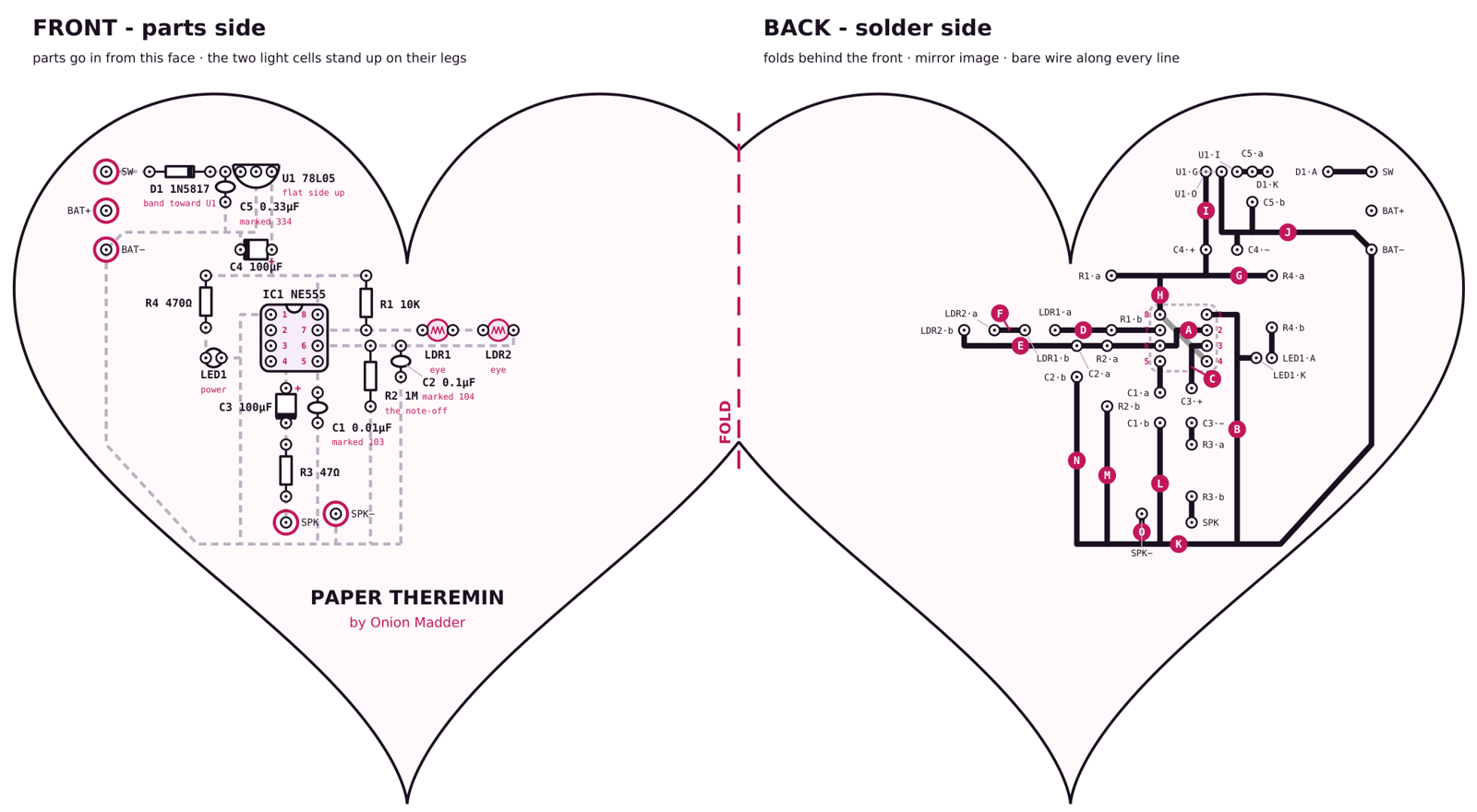
Front: each part is drawn where it sits, with its value printed next to it. The faint dashed lines are only a preview of what connects on the back. The five ringed holes are for wires going off the board: BAT+ and BAT− for the battery, SW for the toggle's return, SPK and SPK− for the speaker.
Back: every bold black line is bare wire or a bent part leg. The lines with a pink letter are bare wire, and the steps name them by that letter; the short unlettered ones are a part's own leg, bent along the line. The gray diagonal is the insulated wire J1. Small pink numbers beside the chip holes are its pin numbers.
Steps 1–11 Print, fold, glue, poke
The sheet is the circuit board, and it's four sheets of paper thick. A plain sheet folded in half and glued to itself makes the core, then the printed hearts fold around the core and glue on, one heart on each face. The back heart is a mirror image of the front, so once it's folded the holes line up on both faces.
Print at 100% / "Actual size". Fit-to-page shrinks it and the holes stop matching the chip's legs.
| Step | Do |
|---|---|
| 1 | Print page 1 on plain printer paper at 100% / Actual size. |
| 2 | Measure the 100 mm bar at the top right of the sheet. If it isn't 100 mm, fix the print scale and print again. |
| 3 | Fold a second, blank sheet of printer paper in half. |
| 4 | Glue-stick the whole inside of the blank sheet, close it, and press it flat. That's the core: two sheets thick. |
| 5 | Fold the printed sheet along the FOLD line, printing on the outside, so the two hearts sit back to back. |
| 6 | Unfold it again and glue-stick the back of the FRONT heart. |
| 7 | Press the core onto the glued back of the FRONT heart. |
| 8 | Glue-stick the back of the BACK heart, fold it over onto the other face of the core, and press it flat. Now it's four sheets thick. |
| 9 | Let the glue set for a few minutes, then cut along the heart outline through all four layers. Don't cut across the FOLD hinge. |
| 10 | Poke the 8 chip holes from the front with an awl or other sharp point, straight down through all four layers. |
| 11 | Poke the other 34 dots the same way. Check the back and open any hole that didn't come all the way through. |
Steps 12–17 Start in the middle: the chip
Everything builds outward from the chip. Each part goes in from the printed front, then on the back its legs bend along their lines and get soldered there.
Quick dabs only. Paper scorches if you sit on it: touch, flow, lift.
| Step | Do |
|---|---|
| 12 | Push the NE555 into the IC1 holes from the front, notch toward the top edge (the drawn notch). |
| 13 | On the back, bend pins 1, 4, 5 and 8 outward slightly so the chip can't fall out. |
| 14 | Insulated white wire J1 from pin 4 to pin 8, corner to corner across the chip. Solder at both pins. |
| 15 | Trace A: bare wire from pin 2 across the middle, under the chip, to pin 6. Solder at pin 2 and pin 6. |
| 16 | Trace B: bare wire from pin 1 out to the side, then straight down to the ground-bus line. Solder at pin 1 only; the far end gets soldered with the bus. |
| 17 | Trace C: bare wire from pin 3 into the middle under the chip, then straight down past pins 4 and 5 to the C3·+ hole. Solder at pin 3. |
Steps 18–21 The two eyes
The photocells stand up on their legs side by side. On the back they sit in series: pin 7 into the first, the first into the second, the second into pin 6.
| Step | Do |
|---|---|
| 18 | LDR1 into LDR1·a and LDR1·b, and LDR2 into LDR2·a and LDR2·b, both standing up on their legs. |
| 19 | Trace D: bare wire from pin 7 along the line through the R1·b hole to LDR1·a. Solder at pin 7 and at LDR1·a. |
| 20 | Trace F: short bare wire from LDR1·b to LDR2·a. Solder at both. |
| 21 | Trace E: bare wire from pin 6 along the line through the R2·a and C2·a holes, then up to LDR2·b. Solder at pin 6 and at LDR2·b. |
Steps 22–28 The timing parts
Each one goes in from the front and solders where its line already runs; the ones that go to ground get a bare wire down to the ground-bus line.
104 is the timing cap and 103 the control-pin cap. Swapped, it squeals up near 48kHz and sounds dead.
| Step | Do |
|---|---|
| 22 | R1, 10K (brown-black-orange): legs into R1·a and R1·b. Solder R1·b where trace D passes. R1·a waits for the 5V line. |
| 23 | R2, 1M (brown-black-green): legs into R2·a and R2·b. Solder R2·a on trace E. |
| 24 | Trace M: bare wire from R2·b straight down to the ground-bus line. Solder at R2·b. |
| 25 | C2, 0.1 µF (marked 104): legs into C2·a and C2·b. Solder C2·a on trace E. |
| 26 | Trace N: bare wire from C2·b straight down to the ground-bus line. Solder at C2·b. |
| 27 | C1, 0.01 µF (marked 103): legs into C1·a and C1·b. Bend C1·a's leg up to pin 5 and solder at both. |
| 28 | Trace L: bare wire from C1·b straight down to the ground-bus line. Solder at C1·b. |
Steps 29–32 Out to the speaker
Pin 3 drives the speaker through a big cap and a 47Ω, with no amp in between.
| Step | Do |
|---|---|
| 29 | C3, 100 µF: long + leg into C3·+, striped leg into C3·−. Solder C3·+ where trace C ends. |
| 30 | R3, 47Ω (yellow-violet-black): legs into R3·a and R3·b. Bend C3·−'s leg down to R3·a and solder at both. |
| 31 | Bend R3·b's leg down to the SPK pad and solder at both. |
| 32 | Trace O: bare wire from the SPK− pad straight down to the ground-bus line. Solder at SPK−. |
Steps 33–40 Power corner: diode and regulator
Power comes in at the top left. D1 only lets current through one way, so a battery clipped on backwards does nothing, and U1 turns the battery into the 5V the theremin was built on.
U1 has to face the right way: flat side toward the top edge. Turned around, the battery goes into its output.
| Step | Do |
|---|---|
| 33 | D1, 1N5817: band end into D1·K, plain end into D1·A. Bend D1·A's leg left to the SW pad and solder at both. |
| 34 | C5, 0.33 µF (marked 334): legs into C5·a and C5·b. |
| 35 | U1, 78L05: legs into U1·I, U1·G and U1·O, with its flat side facing the top edge of the sheet. |
| 36 | On the back, bend D1·K's leg along the line through C5·a to U1·I. Solder at D1·K, at C5·a and at U1·I. |
| 37 | Trace J: bare wire from U1·G down, then left along the line to the BAT− pad. Solder at U1·G and at BAT−. |
| 38 | Bend C5·b's leg down onto trace J and solder. |
| 39 | C4, 100 µF: long + leg into C4·+, striped leg into C4·−. Bend C4·−'s leg up onto trace J and solder. |
| 40 | Trace I: bare wire from U1·O straight down through C4·+ to the 5V line. Solder at U1·O and at C4·+. |
Steps 41–46 The 5V line, the LED and the ground bus
The 5V line runs across above the chip; the ground bus runs down the left curve and along the bottom.
| Step | Do |
|---|---|
| 41 | Trace G: bare wire along the 5V line from the R4·a hole, past trace I, across to R1·a. Solder at R1·a and where trace I meets it. |
| 42 | Trace H: bare wire from pin 8 straight up to the 5V line. Solder at pin 8 and at the line. |
| 43 | R4, 470Ω (yellow-violet-brown): legs into R4·a and R4·b. Solder R4·a on trace G. |
| 44 | LED1: long leg into LED1·A, short leg into LED1·K. Bend R4·b's leg down to LED1·A and solder at both. Bend LED1·K's leg across onto trace B and solder. |
| 45 | Trace K, ground bus: bare wire from the BAT− pad down the left side, around the curve and along the bottom to the end of trace N. Solder at BAT−, at every trace that meets it, and at the far end. |
| 46 | Snip every leg tail that sticks past its joint. |
Steps 47–51 Off the board
The battery clips onto the board, and the toggle and speaker hang off pads on flying leads. Solder each wire on the back.
Leave the battery unclipped until the meter checks.
| Step | Do |
|---|---|
| 47 | Battery snap red (+) to the BAT+ pad. |
| 48 | Battery snap black (−) to the BAT− pad. |
| 49 | A wire from the BAT+ pad to one lug of the SPST toggle. |
| 50 | A wire from the other toggle lug to the SW pad. |
| 51 | The speaker's two leads to the SPK and SPK− pads. |
Steps 52–55 Check, then play
Meter it before you play it. These readings are with the chip in.
| Step | Do |
|---|---|
| 52 | Clip the battery on and toggle on. LED1 should light. |
| 53 | Meter pin 8 to pin 1: 5V, the regulator's output. |
| 54 | Meter pin 4 to pin 1: 5V too. A missing J1 looks exactly like a dead circuit. |
| 55 | Wave a hand over the eyes. Shade either one and the pitch drops; cup both and the note stops dead. |
⚠ If it won't sing
| Meter between | EXPECT (toggle on) |
|---|---|
| BAT+ pad → BAT− pad | battery voltage |
| U1·I → BAT− pad | battery voltage minus about 0.3 V |
| pin 8 → pin 1 | 5V |
| pin 4 → pin 1 | 5V (the reset, held high) |
| Symptom | Check |
|---|---|
| Nothing at all, LED dark | D1 in backwards (the band goes in D1·K), the battery snap reversed, the toggle wires not on BAT+ and SW, or U1 turned around. |
| Nothing at all, LED lit | J1. Pin 4 has to read 5V; a missing reset wire looks exactly like a dead circuit. |
| Silent, but every reading looks healthy | C1 and C2 swapped. 104 is the timing cap, 103 the control-pin cap; backwards it oscillates near 48kHz. |
| Sound, but the light does nothing | The photocell chain or trace A: either traces D, F and E are not bridging pins 7 and 6, or pin 6 is not tied to pin 2. |
| It never cuts out, just sags | R2, the 1M, is missing or not reaching ground through trace M. |
| It cuts out at the slightest shade | R2 is a smaller value than 1M, or one photocell is much darker than the other. |
| Very quiet | Keep R3 in. On paper the 78L05 can only give about 100 mA, so for more volume plug into an amp instead. |
| A thud on power-up, then silence | One of the electrolytics is in backwards. Stripe is minus. |
| Paper scorched or a hole tore | Glue a scrap of paper over the back, re-poke, carry on. It is paper. |
Things to try
- Swap R2 up to 2.2M if you want to work harder for the note-off.
The 555 astable is the classic one from the datasheet; the two-photocell chain and the 1M note-off are how I built mine. The paper-circuit method is Peter Blasser's / Ciat-Lonbarde's. This layout and the words are my own.