Beetleworth
A bass compressor with a blend knob · By Onion Madder · Mess O' Pedals
I designed this one for my friend Ben. It is the Beetle Compressor reworked for bass: the same NE571 doing the squeezing, with a TL072 in front of it so the bass sees a 1M input, and a blend knob that mixes the plain bass back in under the squashed one.
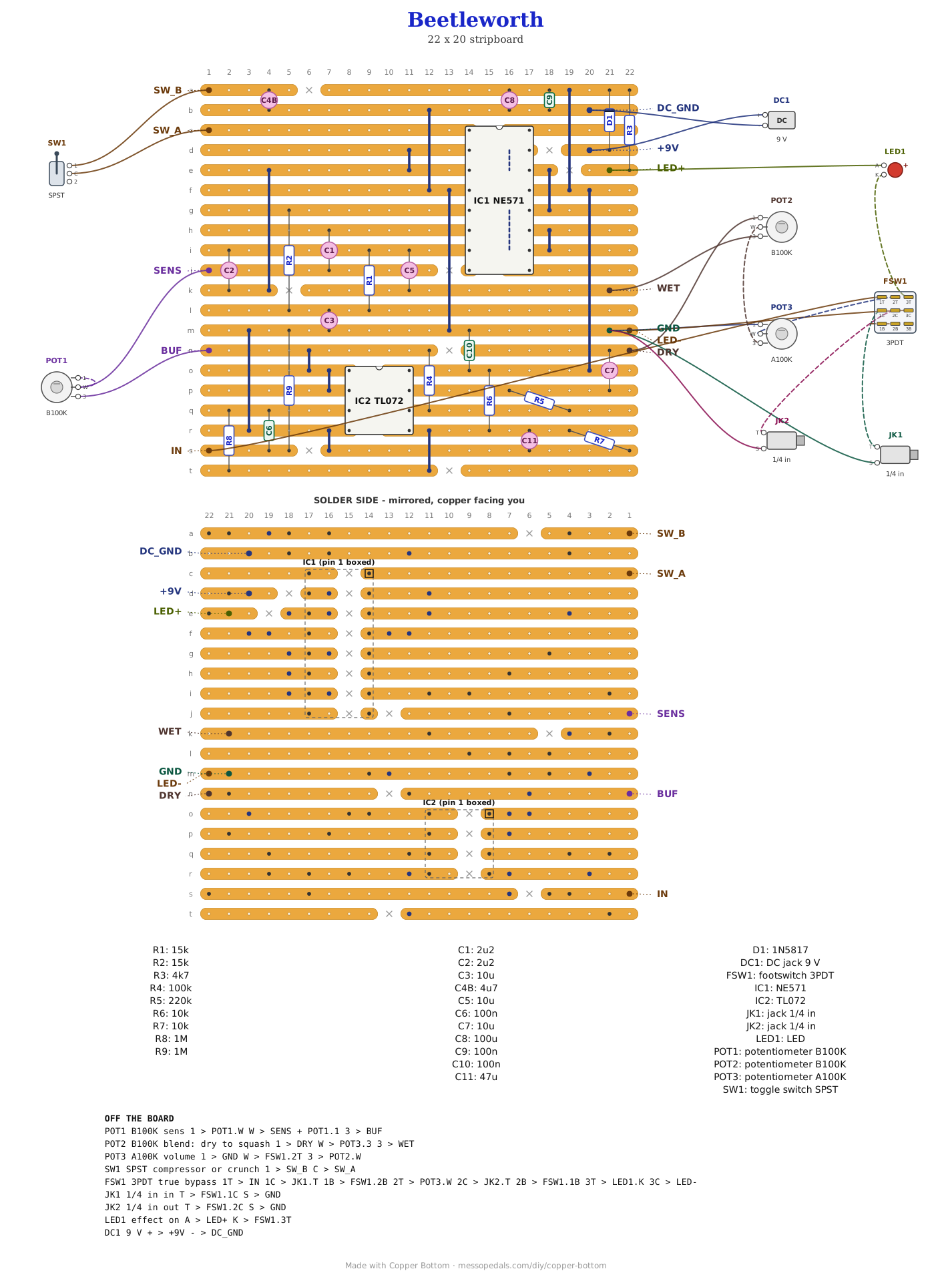
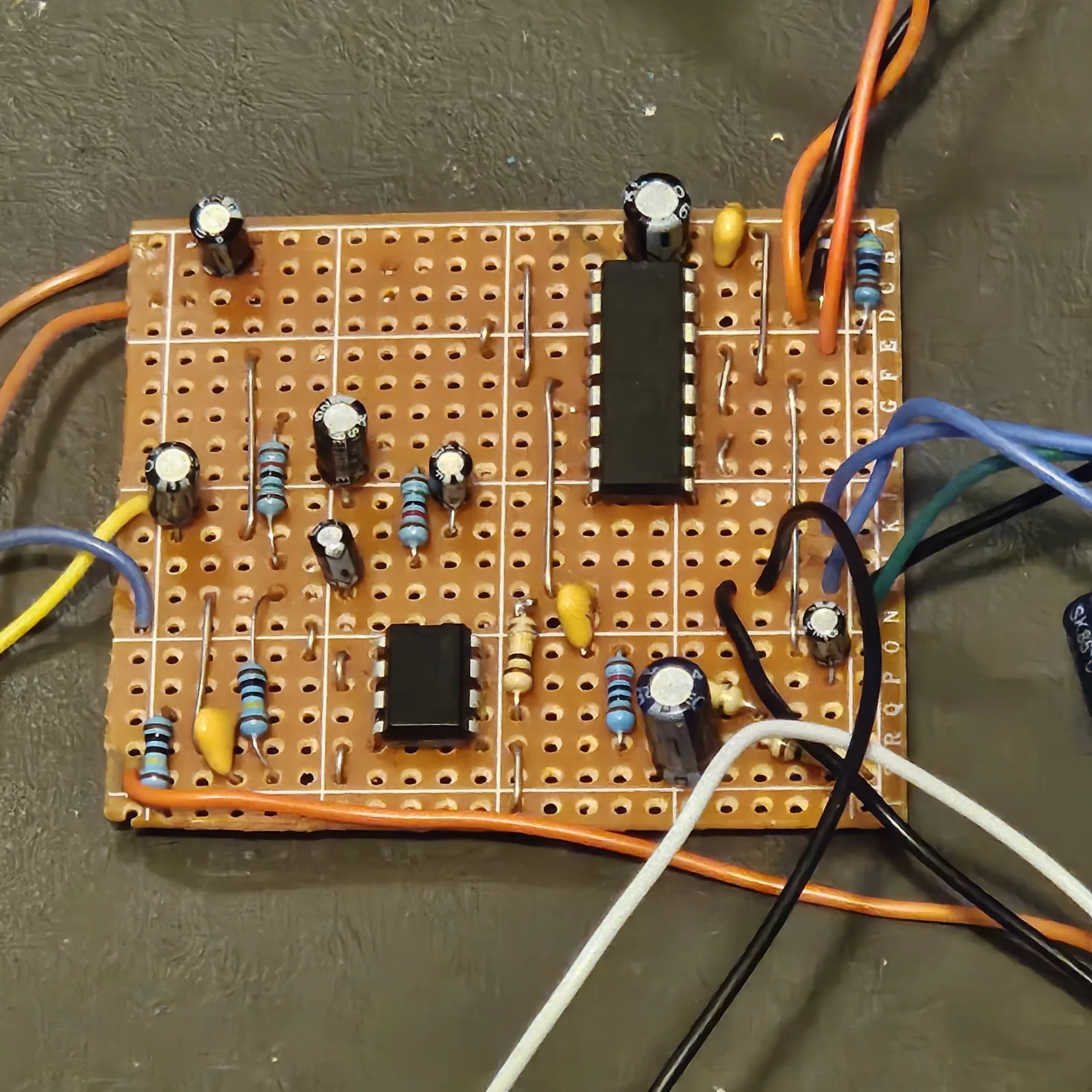
There are three knobs and a toggle. Sens sets how hard the bass hits the compressor, blend goes from dry to squash, and volume sets how much leaves. Beetleworth goes from compressor to crunch with the flip of a switch: business by day and party by night, the perfect pedal for open mic enthusiasts. The toggle does it by taking the capacitor off the chip's level detector. It is a pedal, so there is a footswitch for true bypass, with the LED on it. The board is 20 strips by 22 holes.
What you'll need
tap to expand / collapse
Twenty-one parts on the board plus the two chips and fifteen links, and nine off it.
- 1× NE571 compander, DIP-16 (IC1) - spot it: sixteen legs, NE571 printed on top, a notch or a dot at the pin 1 end. An NE570 or SA571 has the same pins. Only the left-hand half is used. It solders straight to the board
- 1× TL072 dual op-amp, DIP-8 (IC2) - spot it: eight legs, TL072 printed on top, notch at the pin 1 end. One half buffers the input, the other makes the dry side
- 2× 15K resistor (R1, R2) - spot it: bands brown-green-orange. They set where the compressor's output sits
- 2× 10K resistor (R6, R7) - spot it: bands brown-black-orange. They split the supply in half for the TL072. R7 lies at a slant
- 2× 1M resistor (R8, R9) - spot it: bands brown-black-green. R9 holds the input at ground, R8 lifts the buffer to half the supply
- 1× 100K resistor (R4) and 1× 220K resistor (R5) - spot it: brown-black-yellow and red-red-yellow. Together they set how loud the dry side is. R5 lies at a slant
- 1× 4.7K resistor (R3) - spot it: bands yellow-violet-red. It feeds the LED, which is off the board
- 2× 2.2 µF electrolytic (C1, C2) - spot it: a small can with a stripe down one side; the stripe leg is the negative one. C2 feeds the output back to the detector, stripe on strip k. C1 takes the sound in from the sens knob, stripe on strip h
- 1× 4.7 µF electrolytic (C4B) - spot it: the same kind of can. It smooths the chip's level detector, and the toggle switches it in and out. Stripe on strip b
- 3× 10 µF electrolytic (C3, C5, C7) - spot it: a little bigger. C3 steadies the DC feedback, stripe on strip m. C5 is the squashed side's output cap, stripe on strip k. C7 is the dry side's, stripe on strip n
- 1× 47 µF electrolytic (C11) - it steadies the half-supply. Stripe on strip s
- 1× 100 µF electrolytic (C8) - the biggest can, across the supply. Stripe on strip b
- 3× 100 nF capacitor (C6, C9, C10) - spot it: a small box or bead marked 104; it goes in either way. C6 is the input cap, C9 and C10 sit across the supply by each chip
- 1× 1N5817 Schottky (D1) - spot it: fat black body, a gray band at one end. Reverse-polarity protection on the supply; it stands between strips a and d, band on strip a
- 15× wire links - offcuts of component leg. Two of them, J5 and J7, lie under the NE571's body, so they go in before the chip does
Off the board
- 2× B100K linear pot - sens and blend. Sens is a variable resistor: lug 3 to BUF, wiper to SENS, and lug 1 jumpered to the wiper. Blend takes DRY on lug 1 and WET on lug 3, so clockwise is squash, and its wiper goes to volume lug 3
- 1× A100K log pot - volume. Lug 3 from the blend wiper, lug 1 to GND, wiper to the footswitch
- 1× SPST toggle, compressor or crunch - one lug to SW_A, the other to SW_B. Closed is the compressor, open is the crunch
- 1× 3PDT footswitch - true bypass, with the LED on its third pole. The table below has all nine lugs
- 2× 1/4 inch jacks - in on the left, out on the right. Both tips go to the footswitch, both sleeves to GND
- 1× LED - long leg to LED+, short leg to the footswitch. R3 on the board sets its current
- 1× DC jack, 9 V center negative, the usual pedal supply. The sleeve lug is positive and goes to +9V; the center pin is negative and goes to DC_GND. There is no power switch: the footswitch is the bypass, and the pedal is on whenever its supply is plugged in
The layout file is the guide
Like every layout on this shelf, the build document for this one is the file itself: ↓ Download Beetleworth.json - import it into Copper Bottom and the editor gives you the board picture, the placement walkthrough, the electrical checks and a printable build sheet, all from the same file. No coordinates are written out on this page on purpose: the editor is the viewer, and a number typed twice is a number that can drift.
J5 and J7 lie under the NE571, so solder them before the chip goes in. R5 and R7 lie at a slant, each one strip down and three holes across. The input comes in on the left and the two outputs leave on the right, the way the jacks go on my boxes.
Copper Bottom will say one thing, about pin 16. It belongs to the chip's second channel, which this build does not use, and the editor reports it as the only thing on its strip. Leave it empty. The second channel's other pins, 10, 11, 12, 14 and 15, are tied to each other on the board so none of them floats, and pins 8 and 9 are trims the datasheet says may be left open.
The netlist
tap to expand / collapse
I wrote this from the design, and Copper Bottom checks the board against it: every connection it names is on the board and nothing on the board is missing from it. P1, P23 and the rest are named for the NE571's pins. BUF is the buffered bass, VB is half the supply, SWC is the far end of the toggle's capacitor, and CH2 is the unused channel tied to itself.
The off-board wiring
Twelve pads leave the board. Six go to the knobs and the toggle, two to the footswitch, and the rest are power, ground and the LED.
| Pad | Goes to |
|---|---|
| IN | The footswitch, which sends it the input jack tip when the effect is on |
| BUF | Sens pot lug 3 |
| SENS | Sens pot wiper. Jumper lug 1 to the wiper |
| WET | Blend pot lug 3, the clockwise end |
| DRY | Blend pot lug 1. The blend wiper goes to volume pot lug 3, and the volume wiper to the footswitch |
| SW_A / SW_B | The two lugs of the toggle. Closed puts C4B on pin 1, open leaves pin 1 with no capacitor |
| GND | Volume pot lug 1 and both jack sleeves |
| LED+ | The LED's long leg |
| LED- | The footswitch, which joins it to the LED's short leg when the effect is on. Same net as GND |
| +9V / DC_GND | The supply. The jack is center negative: its sleeve lug, the positive, to +9V; its center pin to DC_GND |
The footswitch
This is the usual true bypass on a 3PDT, and Wire a 3PDT Footswitch for True Bypass has the diagram, how to find the columns with a meter and the checks to make afterward. Here is the same wiring with this board's own names. Hold the switch with its nine lugs facing you and the flat sides of the lugs lying crosswise, so they make three columns of three. Each column is one pole: the middle lug is the common, and it connects to the top lug in one position and the bottom lug in the other. Which position is which does not matter, as long as all three columns are wired the same way up.
| Column | Top lug (effect on) | Middle lug | Bottom lug (bypassed) |
|---|---|---|---|
| 1 | The board's IN pad | Input jack tip | A wire across to column 2's bottom lug |
| 2 | Volume pot wiper | Output jack tip | The wire from column 1's bottom lug |
| 3 | The LED's short leg | The board's LED- pad | Empty |
Before you play
Turn the volume down, plug in the power and step on the footswitch: the LED should light. Then meter to ground, with nothing plugged in. These numbers are the datasheets and arithmetic, not off a built board.
| Meter | Expect |
|---|---|
| NE571 pin 13 and TL072 pin 8 | The supply minus about 0.3 V, the drop across D1 |
| TL072 pins 1, 2, 5, 6 and 7 | About half of that, near 4.3 V on a 9 V supply. Pin 3 is the same but sits behind 1M, so a meter reads it a little low |
| NE571 pins 2, 3, 5 and 6 | About 1.8 V each, the chip's own reference, whatever the supply |
| NE571 pin 7 | About 3.6 V, set by R1 and R2. Near 0 V or near the supply: look at R1, R2 and C3 |
How it works, in one breath
The bass comes in through C6 to one half of the TL072, a buffer: it takes almost nothing from the pickups and can drive everything after it. R6 and R7 make half the supply and R8 rests the buffer there, so it can swing both ways on one 9 V supply. From the buffer the sound splits in two.
The squashed side goes out to the sens knob and back in through C1 to the NE571, wired as the Basic Compressor from its datasheet: the chip's gain cell sits in its own op-amp's feedback loop, and C2 points both the gain cell and the level detector at the output. The louder the output gets, the less the op-amp amplifies, so the output grows half as fast as the input in decibels. The sens knob is up to 100K in series with the chip's own 20K input, so turning it down hits the compressor more softly. With the toggle closed, C4B on pin 1 is what the detector averages into, through the chip's own 10K, over about fifty milliseconds, so the squeeze follows the playing and not each cycle of a note. With the toggle open there is no capacitor on pin 1, the squeeze rides the wave itself, and that is the crunch.
The dry side goes through the other half of the TL072, wired by R4 and R5 to turn the signal upside down and make it a little over twice as big. The compressor turns its signal upside down too, so the two sides agree and the blend knob can mix them without one eating the other. The blend wiper feeds the volume knob, and the volume knob feeds the footswitch.
Things to try
None of these have been tried.
- A slower squeeze. C4B at 10 µF makes the compressor side take about a tenth of a second
- A quieter dry side. The dry side is made a little over twice as loud as it came in, and on 9 V the TL072 has about 2.8 V to swing each way, so arithmetic says a bass putting out much over a volt will crunch it. If yours does, R5 at 100K takes the dry side back to the size it came in
- After a fuzz. A compressor after a fuzz evens out its sputter on a fading note
The same circuit on a breadboard
tap to expand / collapse
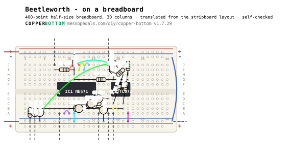
Want to hear it before you solder it? This is the layout file above moved onto a half-size breadboard, 30 columns by Copper Bottom's to breadboard button, in 48 steps with exact holes. It is a translation, not a copy: a strip and a breadboard column are different shapes, so every part is placed fresh and the stripboard's wire links are not needed.
Checked by the app, not built by me. Copper Bottom rebuilt the connections from these holes alone and compared them with the stripboard: all 78 terminals land on the same nets. Nobody has built this breadboard version.
Turn the board so the numbers climb left to right. Then A to E is the lower bank, F to J the upper, the top rails are above J and the bottom rails below A.
The semiconductors
| Step | Do |
|---|---|
| 1 | Seat IC1 (NE571) across the center channel, notch to the LEFT: pin 1 in E8, pin 16 in F8. Pins 1-8 run E8 to E15; pins 9-16 run back F15 to F8. Anywhere in the same bank and column is the same point - E8 and A8 are both pin 1. |
| 2 | Seat IC2 (TL072) across the center channel, notch to the LEFT: pin 1 in E19, pin 8 in F19. Pins 1-4 run E19 to E22; pins 5-8 run back F22 to F19. Anywhere in the same bank and column is the same point - E19 and A19 are both pin 1. |
| 3 | Diode D1 (1N5817): top + rail to H11. The SECOND hole named gets the banded end - the cathode. Backwards, nothing works at all. |
Jumpers
| Step | Do |
|---|---|
| 4 | Jumper: J11 to J19 (IC1.13 to IC2.8). |
| 5 | Jumper: A11 to the bottom − rail (IC1.4 to GND). |
| 6 | Jumper: A22 to the bottom − rail (IC2.4 to GND). |
| 7 | Jumper: A9 to A10 (IC1.2 to C2.B). |
| 8 | Jumper: J9 to J10 (IC1.15 to IC1.14). |
| 9 | Jumper: I10 to J12 (IC1.14 to IC1.12). |
| 10 | Jumper: I12 to J13 (IC1.12 to IC1.11). |
| 11 | Jumper: I13 to J14 (IC1.11 to IC1.10). |
| 12 | Jumper: B19 to A20 (@BUF to IC2.2). |
| 13 | Jumper: A4 to J22 (C11.A to IC2.5). |
| 14 | Jumper: tie the top − rail to the bottom − rail at the right-hand end, so they are one rail. |
Resistors
| Step | Do |
|---|---|
| 15 | Resistor R1 (15k): C14 to C17. |
| 16 | Resistor R2 (15k): C12 to B17. |
| 17 | Resistor R3 (4k7): I11 to I7. |
| 18 | Resistor R4 (100k): C19 to H21. |
| 19 | Resistor R5 (220k): H20 to I21. |
| 20 | Resistor R6 (10k): G11 to G22. |
| 21 | Resistor R7 (10k): H22 to top − rail. |
| 22 | Resistor R8 (1M): C21 to I22. |
| 23 | Resistor R9 (1M): C2 to bottom − rail. |
Ceramics and film
| Step | Do |
|---|---|
| 24 | Cap C6 (100n): B2 to B21. |
| 25 | Cap C9 (100n): H19 to top − rail. |
| 26 | Cap C10 (100n): I19 to top − rail. |
Electrolytics
| Step | Do |
|---|---|
| 27 | Cap C1 (2u2): + leg into C16, − leg into C13. The stripe on the can marks the MINUS leg. Backwards, an electrolytic eventually vents. |
| 28 | Cap C2 (2u2): + leg into B14, − leg into B10. |
| 29 | Cap C3 (10u): + leg into D17, − leg into the bottom − rail. |
| 30 | Cap C4B (4u7): + leg into C3, − leg into the bottom − rail. |
| 31 | Cap C5 (10u): + leg into D14, − leg into D18. |
| 32 | Cap C7 (10u): + leg into I20, − leg into I18. |
| 33 | Cap C8 (100u): + leg into G19, − leg into the top − rail. |
| 34 | Cap C11 (47u): + leg into C4, − leg into the bottom − rail. |
Off-board
| Step | Do |
|---|---|
| 35 | Wire for BUF: into A19. This is where sens pot lug 3 joins the board. |
| 36 | Wire for DRY: into J18. This is where blend lug 1 joins the board. |
| 37 | Wire for IN: into A2. This is where footswitch IN joins the board. |
| 38 | Wire for LED+: into J7. This is where LED anode joins the board. |
| 39 | Wire for SENS: into A16. This is where sens pot wiper (lug 2), with lug 1 jumpered to it joins the board. |
| 40 | Wire for SW_A: into A8. This is where toggle lug 2 joins the board. |
| 41 | Wire for SW_B: into A3. This is where toggle lug 1 joins the board. |
| 42 | Wire for WET: into A18. This is where blend lug 3 (CW = squash) joins the board. |
| 43 | Wire for DC_GND: into the bottom − rail. This is where DC jack center pin (center negative) joins the board. |
| 44 | Wire for LED-: into the bottom − rail. This is where footswitch, which grounds the LED cathode when the effect is on joins the board. |
Power up
| Step | Do |
|---|---|
| 45 | +9V - DC jack sleeve lug (center negative): clip to the top + rail. |
| 46 | GND - jack sleeves + volume lug 1: clip to the bottom − rail. |
| 47 | Before the battery: meter on continuity. rail to rail reads open, not a short J11 to J19 beeps (IC1.13 to IC2.8) A11 to bottom − rail beeps (IC1.4 to GND) A22 to bottom − rail beeps (IC2.4 to GND) A9 to A10 beeps (IC1.2 to C2.B) J9 to J10 beeps (IC1.15 to IC1.14) I10 to J12 beeps (IC1.14 to IC1.12) I12 to J13 beeps (IC1.12 to IC1.11) I13 to J14 beeps (IC1.11 to IC1.10) |
| 48 | Power on. |
Translated by Copper Bottom v1.7.29 from Beetleworth.json.
The compressor is the Basic Compressor from onsemi's NE570 datasheet, the NE571's sibling with the same pins. The rest of the circuit, the layout and the words are mine, and so is anything wrong with them.