Firefly Notebox
A random-note box · By Onion Madder · Mess O' Pedals
This one plays random notes. A fast oscillator runs far too high to hear, and on every tick of a slow clock a switch grabs whatever voltage it happens to be at and holds it. That held voltage sets the pitch of a third oscillator, so every tick is a new note, and an LED blinks with the clock. RATE sets how often the note changes, PITCH sets where the notes land, and there is a volume knob. Three chips on a 12 by 27 board.
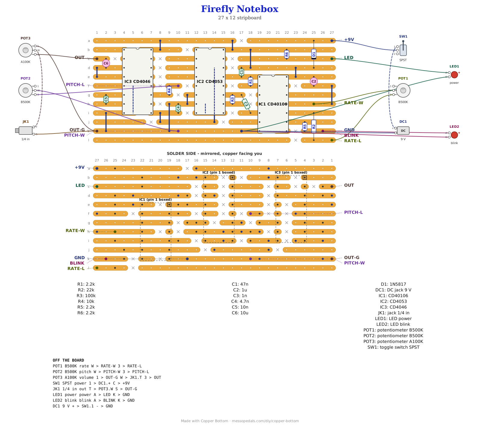
It started as the Paper Firefly, and on paper it sounds chirpy and beepy, and the RATE knob kicks it from slow beeps to whacky noise. This is the same circuit for a box: every part has the same name on both boards. The two LEDs sit on the paper but hang off this board on wires, so the blink can go on the face of the box, with their resistors still on the copper.
What you'll need
tap to expand / collapse
Thirteen parts on the board plus the three chips and thirteen links, and eight off it.
- 1× CD40106 hex Schmitt inverter, DIP-14 (IC1) - spot it: fourteen legs, 40106 printed on top, a notch or a dot at the pin 1 end. It is the fast oscillator and the slow clock. It sits on the right, three strips lower than the other two
- 1× CD4053 triple analog switch, DIP-16 (IC2) - spot it: sixteen legs, 4053 printed on top. One of its three switches does the sampling; the other two are not used, and most of its pins are left empty on purpose
- 1× CD4046 PLL, DIP-16 (IC3) - spot it: sixteen legs, 4046 printed on top. Only its oscillator is used. Pin 15 stays empty: it is a zener inside the chip. All three chips solder straight to the board
- 3× 2.2K resistor (R1, R5, R6) - spot it: bands red-red-red. R1 sets the fast oscillator; R5 and R6 feed the blink LED and the power LED, which are off the board. All three stand up
- 1× 10K resistor (R4) - spot it: bands brown-black-orange. In series with the pitch pot; it stands up on strips f and g
- 1× 22K resistor (R2) - spot it: bands red-red-orange. In series with the rate pot; it lies from strip i down to strip l
- 1× 100K resistor (R3) - spot it: bands brown-black-yellow. It stands up beside C3
- 4× ceramic caps - spot it: a small disc or blob with a three-digit code. C3 is 1 nF (
102), C4 is 4.7 nF (472), C5 is 10 nF (103) and C1 is 47 nF (473). Each one sets something different, so check the print before it goes in - 1× 1 µF electrolytic (C2) and 1× 10 µF electrolytic (C6) - spot it: a small can with a stripe down one side; the stripe leg is the negative one. C2 sets the clock, stripe down on strip f. C6 is the output cap, stripe up on strip c, toward OUT
- 1× 1N5817 Schottky (D1) - spot it: fat black body, a gray band at one end. Reverse-polarity protection on the supply; it stands from strip a down to strip d, band down on strip d
- 13× wire links - offcuts of component leg. Three of them, J1, J7 and J10, run under a chip's body, so they go in before the chips do
Off the board
- 2× B500K linear pots - rate and pitch, two lugs each. Rate: wiper to RATE-W, lug 3 to RATE-L. Pitch: wiper to PITCH-W, lug 3 to PITCH-L. Lug 1 stays empty on both
- 1× A100K log pot - volume. Lug 3 to OUT, lug 1 to OUT-G, wiper to the output jack tip
- 1× 1/4 inch jack - the output. Tip to the volume wiper, sleeve to OUT-G
- 2× LEDs - the blink and the power light. Long legs to BLINK and LED, short legs to GND. R5 and R6 on the board set their current
- 1× DC jack, 9 V center negative
- An SPST toggle for power, in the positive supply lead between the DC jack and the board's +9V pad. Every build on this shelf gets one, and the drawing above shows it
The layout file is the guide
Like every layout on this shelf, the build document for this one is the file itself: ↓ Download Firefly_Notebox.json - import it into Copper Bottom and the editor gives you the board picture, the placement walkthrough, the electrical checks and a printable build sheet, all from the same file. No coordinates are written out on this page on purpose: the editor is the viewer, and a number typed twice is a number that can drift.
J1, J7 and J10 run under the chips, so solder them before the chips go in. J7 takes IC3's pin 5 ground down to pin 8 under its body; J10 joins IC2's two lower ground strips; J1 carries the held voltage from strip j, below IC2, up under its body to pin 14.
Copper Bottom will say ten things, and they are all expected. Eight are pins that are the only thing on their strip: IC2's pins 1 to 5, 12 and 15, the switches this build does not use, and IC3's pin 12, which the 4046 is happy to have left open. The other two say IC1 and IC3 have rows with no cut between their pin columns. Those rows are meant to be joined: on IC1, each unused inverter's input takes the output facing it, and the clock's output faces the input it drives; on IC3, the oscillator's output reaches pins 3 and 14 that way. The Paper Firefly does the same with a wire across each chip.
The netlist
My script wrote this from the design and the board was checked against it in Copper Bottom: every connection it names is on the board and nothing on the board is missing from it. The same script checks every net against the Paper Firefly's, both ways, so the two boards are one circuit. The paper board also runs the held voltage through IC2's pin 3 as a place to solder its one insulated wire; here pin 3 is left empty, which is the only difference. TRI is the fast oscillator, CLK the slow clock, SEL the sample pulse, HOLD the held voltage and VCO the note. The empty pins are not listed.
The off-board wiring
Ten pads leave the board: the rate and pitch pots, the output and its ground, the two LEDs, and the supply.
| Pad | Goes to |
|---|---|
| RATE-W / RATE-L | The rate pot's wiper and lug 3. Lug 1 stays empty. If it runs backwards, move the RATE-L wire to lug 1 |
| PITCH-W / PITCH-L | The pitch pot's wiper and lug 3. Lug 1 stays empty. PITCH-W is ground |
| OUT | Volume pot lug 3. The wiper goes to the output jack tip, and lug 1 to OUT-G |
| OUT-G | Volume pot lug 1 and the output jack sleeve. Same net as GND |
| BLINK | The blink LED's long leg; its short leg to GND |
| LED | The power LED's long leg; its short leg to GND |
| +9V / GND | The supply, through the power toggle. DC jack positive to the toggle and the toggle to +9V; negative to GND |
Before you play
Turn the volume down and switch it on: the power LED should light and the blink LED should blink. Then meter to ground. These numbers are the datasheets and arithmetic, not off a built board.
| Meter | Expect |
|---|---|
| IC1 pin 14, IC2 pin 16, IC3 pin 16 | The supply minus about 0.3 V, the drop across D1 |
| IC1 pin 1 | About half the supply, steady: the fast oscillator running too fast for the meter to follow |
| IC1 pin 10 | Swinging between zero and the supply with the blink, with RATE turned slow |
| IC3 pin 9 | A new value between about 3 V and 5.5 V at each blink, steady between blinks |
How it works, in one breath
IC1's first inverter, R1 and C1 make an oscillator far too high to hear, and the voltage on C1 rises and falls between the chip's two switching thresholds, about a third and two thirds of the supply. Another inverter, R2, the RATE pot and C2 make the slow clock, and a third inverter after it drives the blink LED. On every rising clock edge, C3 and R3 make a spike tens of microseconds long on IC2's select pin, and for that instant the switch joins C1's voltage to C4. When the spike ends the switch opens and C4 keeps what it grabbed.
That held voltage goes into the CD4046's oscillator on pin 9, so it plays a note, with C5, R4 and the PITCH pot setting where the notes sit. Since the held voltage always lands between a third and two thirds of the supply, every note falls within about eight semitones of where PITCH puts them. C6 takes the DC off the output and the volume pot sets how much leaves.
Things to try
None of these have been tried on this board, and none on the paper one either.
- Wider leaps. R4 smaller lets each note jump further, but keep it 10K or more
- A photocell for RATE. An LDR in place of the rate pot, across RATE-L and RATE-W, and the notes speed up in the light
- Into a ring mod. Random notes against a steady drone, through the XOR Ring Mod
Sample-and-hold random notes from a fast oscillator and a slow clock is an old synth trick, and the 40106 oscillator and the 4046 VCO are out of every CMOS cookbook. The layout and the words are mine, and so is anything wrong with them.