Moth
MN3207 chorus and vibrato · By Onion Madder · Mess O' Pedals
A chorus that turns into a vibrato on one toggle. An MN3207 bucket-brigade chip delays the guitar by a few milliseconds and a slow wave stretches and shrinks that delay, so the copy wobbles in pitch. Mixed with the dry signal it is a chorus: wide and shimmery. Alone it is a vibrato: the note itself bends.
An MN3207 usually gets its clock from a companion chip, the MN3102. My drawers have no MN3102, so this one builds the clock out of chips that are there: a CD4046 makes the frequency and a CD4013 splits it into the two opposite square waves the delay chip needs.
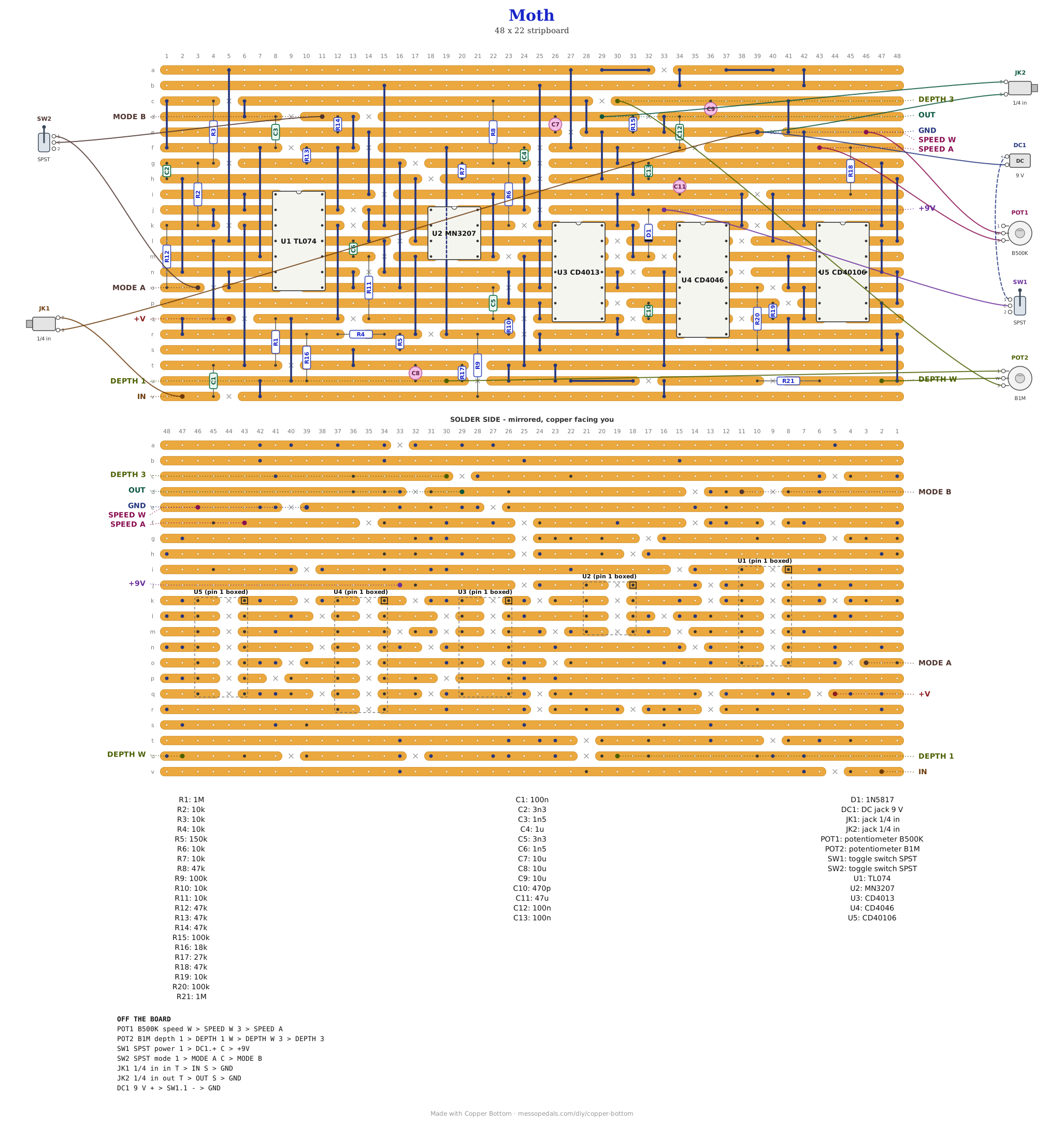
What you'll need
tap to expand / collapse
Five chips, 35 small parts and 66 wire links on the board. It is a big board and a lot of links: take them a strip at a time from the walkthrough in Copper Bottom. Every chip solders straight to the board.
- 1× MN3207 bucket-brigade delay, DIP-8 (U2) - spot it: eight legs, MN3207 on top; a BL3207 or V3207 is the same chip from another maker. It is the delay
- 1× CD4046 phase-locked loop, DIP-16 (U4) - spot it: sixteen legs, CD4046 or HEF4046 on top. Only its VCO is used: it makes the clock
- 1× CD4013 dual D flip-flop, DIP-14 (U3) - spot it: fourteen legs, CD4013 on top. It halves the clock into its two opposite phases
- 1× CD40106 hex Schmitt inverter, DIP-14 (U5) - spot it: fourteen legs, CD40106 or HEF40106 on top. It is the slow sweep
- 1× TL074 quad op-amp, DIP-14 (U1) - spot it: fourteen legs, TL074 on top. The input buffer, the two filters and the mix
- Resistors: 8× 10K (R2, R3, R4, R6, R7, R10, R11, R19), 5× 47K (R8, R12, R13, R14, R18), 3× 100K (R9, R15, R20), 2× 1M (R1, R21), and one each of 18K (R16), 27K (R17) and 150K (R5) - spot them: 10K brown-black-orange, 47K yellow-violet-orange, 100K brown-black-yellow, 1M brown-black-green, 18K brown-gray-orange, 27K red-violet-orange, 150K brown-green-yellow
- Film capacitors: 2× 3.3nF (C2, C5), 2× 1.5nF (C3, C6), 100nF (C1) and 1µF (C4) - spot them: printed 332, 152, 104 and 105. The 3.3n and 1.5n pairs are the two filters
- Ceramic capacitors: 470pF (C10, printed 471), the VCO's timing cap, and 2× 100nF (C12, C13, printed 104) on the supply
- Electrolytics: 3× 10µF (C7, C8, C9) and 47µF (C11) - spot them: small cans with a stripe down the negative side; the file shows which way each goes
- 1× 1N5817 Schottky (D1) - spot it: fat black body, gray band. It stops a supply plugged in backwards
- 66× wire links - offcuts of component leg. One runs under U2 from end to end, down the middle between its two rows of legs; that is ordinary
Off the board
- 1× B500K linear pot - SPEED, wiper and lug 3; lug 1 stays empty
- 1× B1M linear pot - DEPTH, all three lugs
- 1× SPST toggle - MODE: closed is chorus, open is vibrato
- An SPST toggle for power, in the supply's plus lead before the board's +9V pad. Every build on this shelf gets one, and the drawing above shows it
- 2× 1/4 in jacks - in and out
- 1× 2.1 mm DC jack for a 9 V center-negative pedal supply
- A box with room for two knobs, two toggles and three jacks. Nobody has drawn a drill template for this one yet
The layout file is the guide
Like every layout on this shelf, the build document is the file: ↓ Download Moth.json - import it into Copper Bottom and the editor gives you the board picture, the placement walkthrough, the electrical checks and a printable build sheet, all from the same file. No coordinates are written out on this page on purpose: the editor is the viewer, and a number typed twice is a number that can drift.
Four rows under the chips have no cut, three under the CD4013 and one under the CD4046, where the two pins facing each other are both ground: the strip runs under the chip and joins them, on purpose. The cuts go in before the links, because several links lie over cut holes. The chips go in last: solder everything else, do the meter check below, then the chips.
The netlist
My script wrote this from the design and checked the board against it, and so did Copper Bottom: every connection the netlist names is on the board and nothing on the board is missing from it. Twelve chip pins are left empty on purpose, so the netlist does not mention them: the CD4013's second pair of outputs, the parts of the CD4046 that are not its VCO, and five of the CD40106's six outputs.
The off-board wiring
| Pad | Goes to |
|---|---|
| +9V | DC jack +, through the power switch |
| GND | DC jack -, both jack sleeves |
| +V | a test pad on the supply after D1; nothing else |
| IN | input jack tip |
| OUT | output jack tip |
| SPEED A | SPEED pot lug 3 (lug 1 empty) |
| SPEED W | SPEED pot wiper (lug 2) |
| DEPTH 1 | DEPTH pot lug 1: the bias, the no-sweep end |
| DEPTH W | DEPTH pot wiper (lug 2): into the VCO |
| DEPTH 3 | DEPTH pot lug 3: the LFO |
| MODE A | MODE toggle (SPST), one lug: closed is chorus (dry and wet), open is vibrato (wet only) |
| MODE B | MODE toggle (SPST), the other lug |
First power-up
- Before the chips go in. Plug in the 9 V supply, switch on, and check for about 8.7 V from the GND pad to the +V pad, and to each chip's supply hole: U1 pin 4, U2 pin 5, U3 pin 14, U4 pin 16 and U5 pin 14
- Still before the chips: about 5.2 V on the DEPTH 1 pad (the bias everything sits on), and about 8.1 V at U2 pin 4, the delay chip's gate bias
- Switch off, solder the five chips in, notch the way the file shows, and switch on. U2 pins 2 and 6, the two clock phases, should each read about half the supply on a meter, because they are square waves switching too fast for it to follow
- Plug in a guitar and an amp. With MODE closed and DEPTH and SPEED halfway, it should shimmer. Open MODE for vibrato
How it works, in one breath
The TL074's first op-amp buffers the input, and its second is a low-pass filter at about 7 kHz that feeds the MN3207, sitting on a 5.2 V bias, where Panasonic's curve puts the delay chip's lowest distortion for this supply. The MN3207 passes the signal along 1024 stages, two clock ticks a step, so the delay is 512 clock periods. The clock comes from the CD4046's VCO, which runs at about 140 kHz with its control pin on the bias, halved by the CD4013 into two opposite square waves at about 70 kHz: a delay of about 7 ms. The CD40106 is a slow oscillator, about a quarter of a cycle a second to nearly three, and DEPTH feeds some of it to the VCO, so the delay swings from about 6 to 9 ms. The two outputs of the MN3207 are added through R6 and R7, which cancels most of the clock, the TL074's third op-amp filters off the rest, and its fourth adds the delayed copy to the dry signal, or alone when MODE is open. All of that is arithmetic from the datasheets.
One thing to know before building. Panasonic's sheet asks for the two clock phases to cross below 30% of the supply, which its own clock chip does. A CD4013's two outputs cross near half the supply instead. Plenty of builds clock a bucket-brigade chip from a flip-flop like this, but it is outside the sheet, and this one is untested.
Things to try
None of these have been tried, because none of this has.
- A flanger. C10 at 220pF roughly doubles the clock and halves the delay, toward 3 to 4 ms. Add a wire from the wet side back into the input for the metallic flanger sound; that needs its own resistor and is not drawn
- A trimmer for the bias. Panasonic adjusts the delay chip's bias for the least distortion. R16 and R17 could become a 50K trimmer between two 10Ks
- Slower. C9 at 22 µF halves the SPEED range, for a slow seasick wobble
The delay chip and its hook-up follow Panasonic's MN3207 data sheet; the clock from a CD4046 and a CD4013 stands in for the MN3102 my drawers do not have. The layout was drawn for this site, and anything wrong with it is mine to fix.