Termite
A shift-register noise box · By Onion Madder · Mess O' Pedals
A noise box from two logic chips. A shift register passes bits along on every tick of a clock, and an XNOR gate feeds two of them back in, so the pattern repeats every 127 ticks. Slow, that is a chattering rhythm of clicks; fast, it turns into a buzz. PITCH sets the clock and there is a volume knob. Two chips on a 12 by 29 board.
It started as the Paper Termite, and on paper it is really cool: a really neat range, from clicks to a sort of machine buzz or whine. This is the same circuit for a box: every part has the same name on both boards. The power LED sits on the paper but hangs off this board on a wire, so it can go on the face of the box, with its resistor still on the copper.
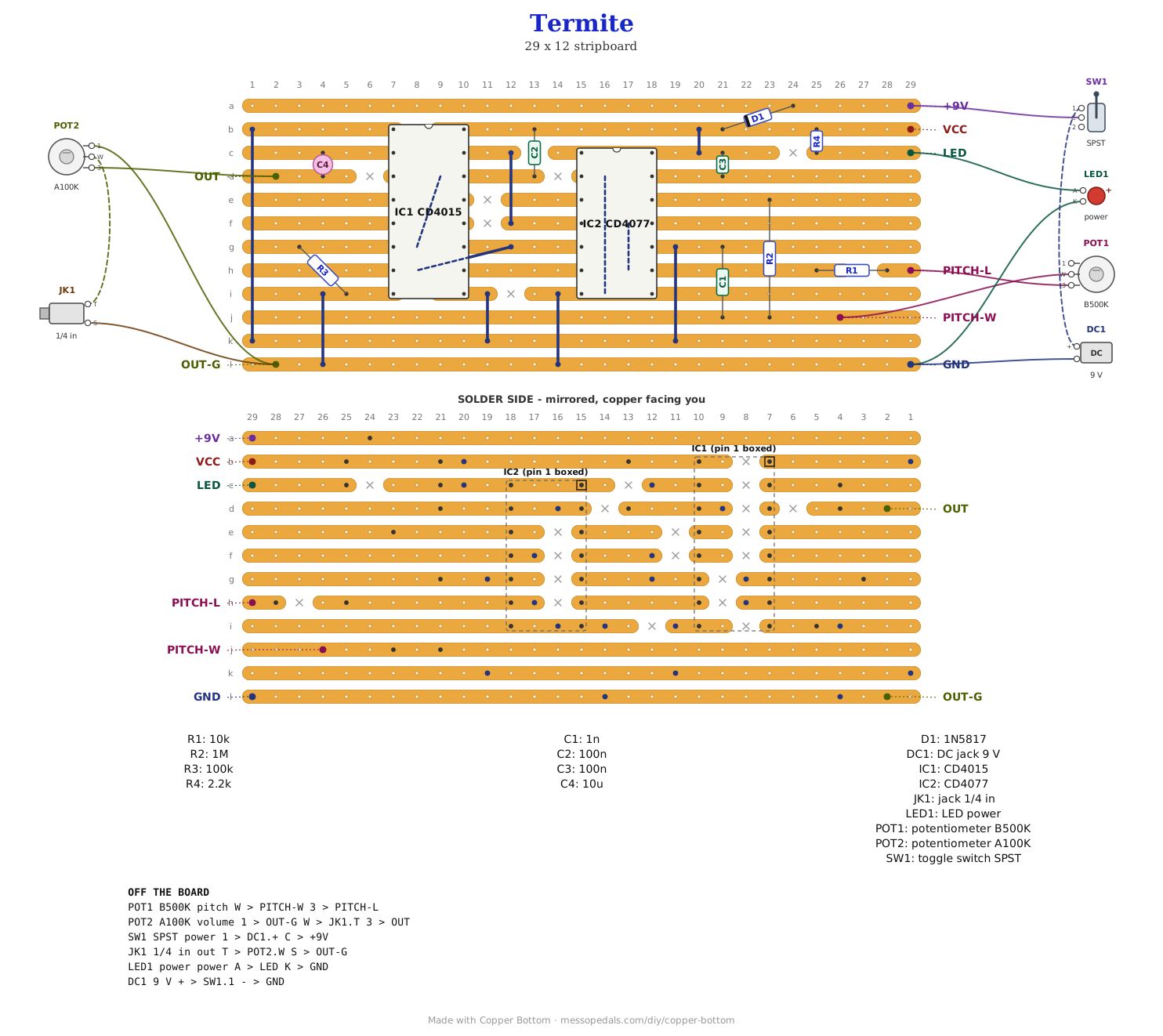
What you'll need
tap to expand / collapse
Nine parts on the board plus the two chips and eleven links, and six off it.
- 1× CD4015 dual 4-stage shift register, DIP-16 (IC1) - spot it: sixteen legs, 4015 printed on top, a notch or a dot at the pin 1 end. It sits on the left. Pins 3, 4, 5, 12 and 13 are outputs this build does not use, and stay empty on purpose
- 1× CD4077 quad XNOR, DIP-14 (IC2) - spot it: fourteen legs, 4077 printed on top. A 4070 is XOR, not XNOR, and will not do: check the print. It sits on the right, one strip lower. Both chips solder straight to the board
- 1× 2.2K resistor (R4) - spot it: bands red-red-red. It feeds the power LED, which is off the board, and stands up near the top right
- 1× 10K resistor (R1) - spot it: bands brown-black-orange. In series with the pitch pot; it lies along strip h
- 1× 100K resistor (R3) - spot it: bands brown-black-yellow. Half of the power-on reset; it lies on the slant left of IC1
- 1× 1M resistor (R2) - spot it: bands brown-black-green. Part of the clock; it lies from strip e down to strip j
- 3× ceramic caps - spot it: a small disc or blob with a three-digit code. C1 is 1 nF (
102) and sets the clock's range; C2 and C3 are 0.1 µF (104). C2 is the other half of the power-on reset, C3 sits across the supply beside IC2 - 1× 10 µF electrolytic (C4) - spot it: a small can with a stripe down one side; the stripe leg is the negative one. It is the output cap, stripe down on strip d, toward OUT
- 1× 1N5817 Schottky (D1) - spot it: fat black body, a gray band at one end. Reverse-polarity protection on the supply; it lies on the slant from strip a to strip b, band on strip b
- 11× wire links - offcuts of component leg. Four of them, J1 and J2 under IC1 and J7 and J9 under IC2, run under a chip's body, so they go in before the chips do. J1 and J2 are diagonals: use insulated hookup wire for those two
Off the board
- 1× B500K linear pot - pitch, two lugs. Wiper to PITCH-W, lug 3 to PITCH-L. Lug 1 stays empty
- 1× A100K log pot - volume. Lug 3 to OUT, lug 1 to OUT-G, wiper to the output jack tip
- 1× 1/4 inch jack - the output. Tip to the volume wiper, sleeve to OUT-G
- 1× LED - the power light. Long leg to LED, short leg to GND. R4 on the board sets its current
- 1× DC jack, 9 V center negative
- An SPST toggle for power, in the positive supply lead between the DC jack and the board's +9V pad. Every build on this shelf gets one, and the drawing above shows it
The layout file is the guide
Like every layout on this shelf, the build document for this one is the file itself: ↓ Download Termite.json - import it into Copper Bottom and the editor gives you the board picture, the placement walkthrough, the electrical checks and a printable build sheet, all from the same file. No coordinates are written out on this page on purpose: the editor is the viewer, and a number typed twice is a number that can drift.
J1, J2, J7 and J9 run under the chips, so solder them before the chips go in. Under IC1, J1 takes the reset from pin 14 across to pin 6, and J2 takes the loop from pin 11 across to pin 7, passing between pins 10 and 11 on its way. Under IC2, J7 joins pins 11 and 9, the clock's first gate, and J9 joins the ground strips at pins 2 and 13 to the one at pins 7 and 8.
Copper Bottom reports this one clean. The VCC pad is a test point for a meter, there so the checker knows that strip is the supply; nothing is wired to it.
The netlist
My script wrote this from the design and the board was checked against it in Copper Bottom: every connection it names is on the board and nothing on the board is missing from it. The same script checks every net against the Paper Termite's, both ways, so the two boards are one circuit. CLK is the clock, N1 and OSC the clock's two gates, JUNC the point where its timing parts meet, FB the XNOR fed back into the second register, Q3B and Q4A the two stages it feeds back from, and QOUT the sound. The empty pins are not listed.
The off-board wiring
Seven pads leave the board, and one of them, VCC, is only a test point: the pitch pot, the output and its ground, the LED, and the supply.
| Pad | Goes to |
|---|---|
| PITCH-W / PITCH-L | The pitch pot's wiper and lug 3. Lug 1 stays empty. If it runs backwards, move the PITCH-L wire to lug 1 |
| OUT | Volume pot lug 3. The wiper goes to the output jack tip, and lug 1 to OUT-G |
| OUT-G | Volume pot lug 1 and the output jack sleeve. Same net as GND |
| LED | The power LED's long leg; its short leg to GND |
| +9V / GND | The supply, through the power toggle. DC jack positive to the toggle and the toggle to +9V; negative to GND |
| VCC | Nothing. A test point: the supply after D1 |
Before you play
Turn the volume down and switch it on: the power LED should light. Then meter to ground. These numbers are the datasheets and arithmetic, not off a built board.
| Meter | Expect |
|---|---|
| The VCC pad, IC1 pin 16, IC2 pin 14 | The supply minus about 0.3 V, the drop across D1 |
| IC1 pin 6 | Zero, once the power has been on for a moment |
| IC2 pin 10 | About half the supply: a meter reads a running clock that way. Zero or the full supply means the clock is stopped |
| IC1 pin 2 | Somewhere near half, and wandering |
If it plays one steady click or tone that never changes pattern, the register is stuck: power off, wait a few seconds and power on. If it sticks again, meter IC1 pin 6, which should be zero, and look at R3, C2 and J1.
How it works, in one breath
Two of IC2's XNOR gates, each with one input grounded so it acts as an inverter, make the clock with C1, R1, R2 and the PITCH pot. By arithmetic it runs from about 900 Hz to about 45 kHz across the knob. IC1 is two four-stage shift registers clocked together. The third stage of the second one goes back into the first one's data input, and another of IC2's gates, the XNOR of that stage and the first register's fourth, goes into the second one's, so the bits run round a loop of seven stages that comes back to where it started every 127 ticks.
The sound is the last stage, IC1 pin 2, through C4 to the volume pot. The one pattern that never moves is all ones, so C2 and R3 hold both resets high for a moment at power-on and the loop always starts from zeros.
Things to try
None of these have been tried on this board, and none on the paper one either.
- A photocell for the pitch pot. An LDR across PITCH-L and PITCH-W, the way I ran the Hive Drone, and the noise follows your hand
- Slower. C1 at 10 nF (
103) moves the whole range down by ten, so the bottom of the knob is a slow, clicky sequence - Into a ring mod. The Termite on one input and an oscillator on the other, through the XOR Ring Mod
A shift register with XOR feedback is the classic way to make noise from logic chips, and the two-gate RC clock is out of every CMOS cookbook. The layout and the words are mine, and so is anything wrong with them.