16 Step Sequencer (+/-9V to +/-15V)
Article by Ray Wilson · Music From Outer Space · musicfromouterspace.com
This is an intermediate to advanced project and I do not recommend it as a first project if you are just getting started in synths or electronics. Only the circuit and some explanation are shown here. A lot of project building, troubleshooting and electronics experience is assumed. Additionally, electronic equipment ownership (scope, meters, etc.) is taken for granted. If you are interested in building this project please read the entire page before ordering PC boards to ensure that the information provided is thorough enough for you to complete the project successfully.
Digital board redesign eliminates need for previous version's kludges.
Previous Version for Reference (on Ray's original site)
Not Ray's words: this is the 2006 version of the sequencer, the one with the improved digital board, and every drawing below is rendered sharp from Ray's own PDFs rather than his small preview images. Each drawing opens full size when you click it, and the PDF link under it is the original file. The PDFs are drawn at actual size: the board outlines in his two parts layouts measure exactly the 6.30" x 3.30" and 5.50" x 2.60" printed on them. Print them at 100% (not "fit to page"), and check a print against a ruler before anyone drills a panel or a case.
Watch Thomas White's Excellent Sequencer Videos on YouTube
- http://www.youtube.com/watch?v=EU6d24_eZ08
- http://www.youtube.com/watch?v=AvZi-YMvHRE
- http://www.youtube.com/watch?v=s5cx6Z7wDOg
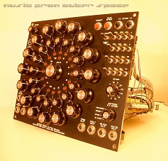
Thomas White used the MFOS sequencer boards to produce this incredible rotary sequencer. Visit his site to keep up with his latest awesome projects.
MP3 Samples
(The recordings live on Ray's site.)
- Reverse At Step Demo
- Reset At Step Demo
- Stop At Step and External Start Demo
- Gate Switch Demo (Gate switch setting are changed throughout)
- Dry Random Demo
- Wet Random Demo with two ocscillators
- Cool Sequence Demo
Features
- Improved PC board (far less kludging)
- Produces sequences of 4 to 16 steps in length
- Modes include stop at count, reverse at count, reset at count and random 16 mode
- Each step has coarse tune, fine tune, and switchable gate
- Accepts external clock and external start pulse.
- Simultaneous outputs with and without portamento.
- Forward, Back, and Reset controls ease sequence set up.
- Approximate current consumption: +12V (21.7 mA) -12V (10.5mA)
Introduction
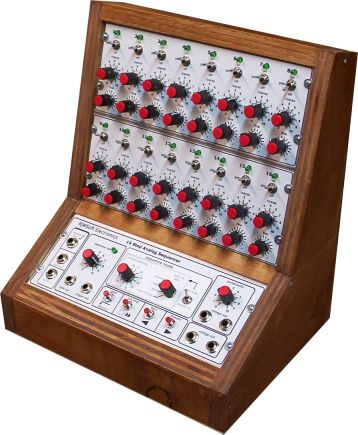
The main idea of a sequencer is to provide an automatic means of sequentially stepping through a series of adjustable voltages to drive a VCO (or any other voltage controlled device). Additionally, gate and trigger signals are generated at the moment the output of the circuit steps to a new voltage. Typically you use a sequencer to control the frequency of an oscillator (or several oscillators) to produce repeating tonal patterns, or arpeggios, which are further enhanced by filtering, modulation, addition of keyboard voltage etc. Sequencers are often used in electronic music production. This sequencer can produce a 4 to 16 note sequence. Additionally, this sequencer provides forward only, forward and back, and the unique ability for random sequencing. The gate/trigger can be included or not at each step (via a switch) and each step has coarse and fine voltage adjustment. Two circuit boards are required for this sequencer (unless you design your own) and I am offering both of them for sale. The digital board drives the sequencer and the analog board switches the control voltage from each set of coarse and fine pots to the output. You can start and stop the sequencer, reset it and step forward and/or backward to set up or manually walk through a sequence.
NEW! Adding More Analog Sequencer PCBs
16 Step Sequencer Schematic Page 1
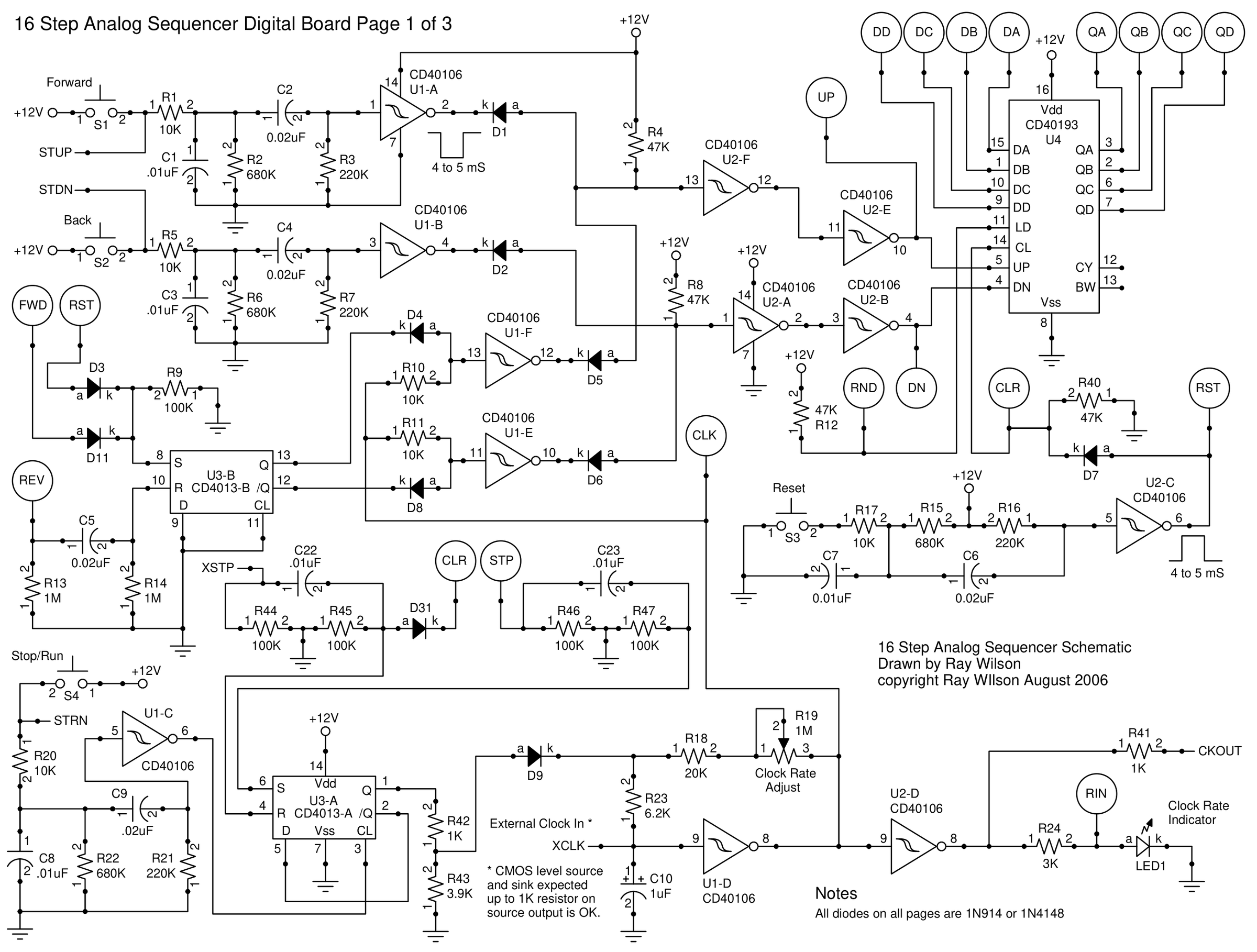
Page 1 shows the clocking and counting section of the circuit. This part of the circuit controls the manual and automatic stepping of the sequencer. U4 counts up when a positive going edge is applied to its UP input while its DN input is held high. Conversely it counts down when a positive going edge is applied to its DN input while the UP input is held high. If the LD input is brought low the outputs of U4 (QA through QD) follow the data on the load inputs (DA through DD). When the sequencer is not in Random mode the LD input is held high via R12 to +12V. A high level on the CL input of U4 causes the counter to reset to a count of zero.
S1 and associated components (R1, C2, C1, R2, R3, and U1-A) comprise a switch debouncer/low going pulser. When S1 is pressed a clean low going pulse of about 1 to 2 mS appears at the output of U1-A. In the same manner, S2 and its associated components and S4 and its associated components form switch debouncer/low going pulsers. S3 and its associated components work in the opposite fashion of S1, S2 and S4 in that when S3 is pressed a clean positive going pulse appears at U2-C pin 6. S3 is used soley to reset counter U4.
The clock (square wave oscillator) for the sequencer is made up of U1-D, C10, R23, R18, and R19 (clock rate adjust). It runs when U3-A's Q output is low thus reverse biasing D9. Due to U1-D being a schmidt trigger inverter it can be made to oscillate by applying its output back to its input via a resistor and connecting a capacitor to its input. When the output is high it charges C10 via R19, R18, and R23 in series until its high threshold is reached at which time its output snaps low and C10 discharges through the same path until U1-D's low threshold is reached when its output snaps high and begins the cycle anew. The purpose of the value changes needed for the clock input modification is to raise the impedance of the external clock input node so that external clocking from sources with output impedance up to 1K can reliably clock the sequencer. A clean rectangular clock source oscillating between ground and +V is assumed. If an external clock source with negative voltage excursions is used then a diode must be placed between the input jack and pin 9 of U1-D. The anode of the diode goes to the jack's hot and the cathode goes to pin 9 of U1-D.
If U3-A's Q output is high the clock is stopped (due to C10 being held fully charged via D9) and its output (U1-D pin 8) is forced low. Pressing S4 toggles the state of U3-A's Q output since U3-A is wired as a divide by two counter. Thus you can start or stop the clock by pressing S4.
The clock signal is fed to the inputs of U1-F and U1-E via 10K resistors R10 and R11 respectively. D4 and D5 are used (in conjunction with U3-B) to control which of these inverters propogate the clock signal.
U3-B is used to control the direction in which U4 counts. When the clock is running and U3-B's Q is high (and subsequently its NOT-Q is low) the clock pulses are allowed to propogate through U1-F but are stopped from passing through U1-E due to U1-E's pin 11 being pulled low via D8.
When the clock is running and U3-B's Q is low (and subsequently its NOT-Q is high) the clock pulses are allowed to propogate through U1-E but are stopped from passing through U1-F due to U1-F's pin 13 being pulled low via D4.
During operation U3-B's set and reset lines are pulsed appropriately to control the count direction.
Notice that the anodes of D5 and D1 are connected to U2-F's input (pin 13). If either U1-A pin 2 or U1-F pin 12 go low then U2-F pin 13 is pulled low (via D1 or D5 respectively). When both U1-A pin 2 and U1-F pin 12 are high, U2-F pin 13 is held high via R4 (47K to +12V). Thus a push of S1 or a low to high transition of U1-F pin 12 can cause U4 to count up. Also note that U2-E pin 10 follows the state of U2-F's input (pin 13).
Notice that the anodes of D2 and D6 are connected to U2-A's input (pin 1). If either U1-B pin 4 or U1-E pin 10 go low then U2-A pin 1 is pulled low (via D2 or D6 respectively). When both U1-B pin 4 or U1-E pin 10 are high, U2-A pin 1 is held high via R8 (47K to +12V). Thus a push of S2 or a low to high transition of U1-E pin 10 can cause U4 to count down. Also note that U2-B pin 4 follows the state of U2-A's input (pin 1).
Normally the UP and DN inputs of U4 are held high. Low to high transitions are used on either UP or DN (while the opposite input is held high) to cause clocking in either direction. When the sequencer is running (i.e. U3-A's Q is high and neither "Step Up" or "Step Down" are being pressed) and U3-B's Q output is high (counting up) U4's DN clock input (pin 4) is held high (as explained above). Thus the counter counts up. This continues until the count is reached that corresponds with the setting of S9 (SP12T selector switch).
Notice that U5 CD4514 (4-bit Latch/4-16 Line Decoder) is controlled by the counter (U4). The output that corresponds to the current counter's QA-QD outputs (one of S-0 through S-15) is high while all of the others are low. U5's outputs S-4 through S-15 are connected to the poles of S9 (S-4 to 1, S-5 to 2, S-6 to 3 through S-15 to 12). This is to allow the sequence to reset or reverse at the set step count. The common pole of S9 is controlled via switches S12, S15, and S16 to connect to:
- Nothing (Random 16 or 16 Step Sequence is selected)
- REV (Reverse count direction when selected step is reached)
- CLR (Zero (or clear) count when selected step is reached)
Notice that any time the S-0 output of U5 goes high that U3-B is set (count up is set). This is so the counter starts to count up anytime the 0th count is reached.
Thus if the sequencer is in "Reverse At Count" mode the sequencer will count up to the step setting of S9 and then reverse direction and count down toward 0. This is because the high going level seen at the REV connection is used to flip U3-B into the state that causes the counter to count down (U3-B's Q is low and U3-B's NOT-Q is high). When 0 is reached the count direction is set to up again. This cycle continues as the sequencer counts up and down until the mode is changed or the clock is stopped.
If the sequencer is in "Reset At Count" mode the sequencer will count up to the step setting of S9 and then clear the counter to zero. The sequencer will continue to count from zero to count and reset until the mode is changed or the clock is stopped.
"16 Step Sequence" mode is provided to allow the sequencer to repeat all 16 steps until the mode is changed or the clock is stopped.
"Random 16" mode causes the counter to assume the count provided at the outputs of U8 CD4094 8 Channel Shift Register/Latch. The random counter is explained below.
16 Step Sequencer Schematic Page 2
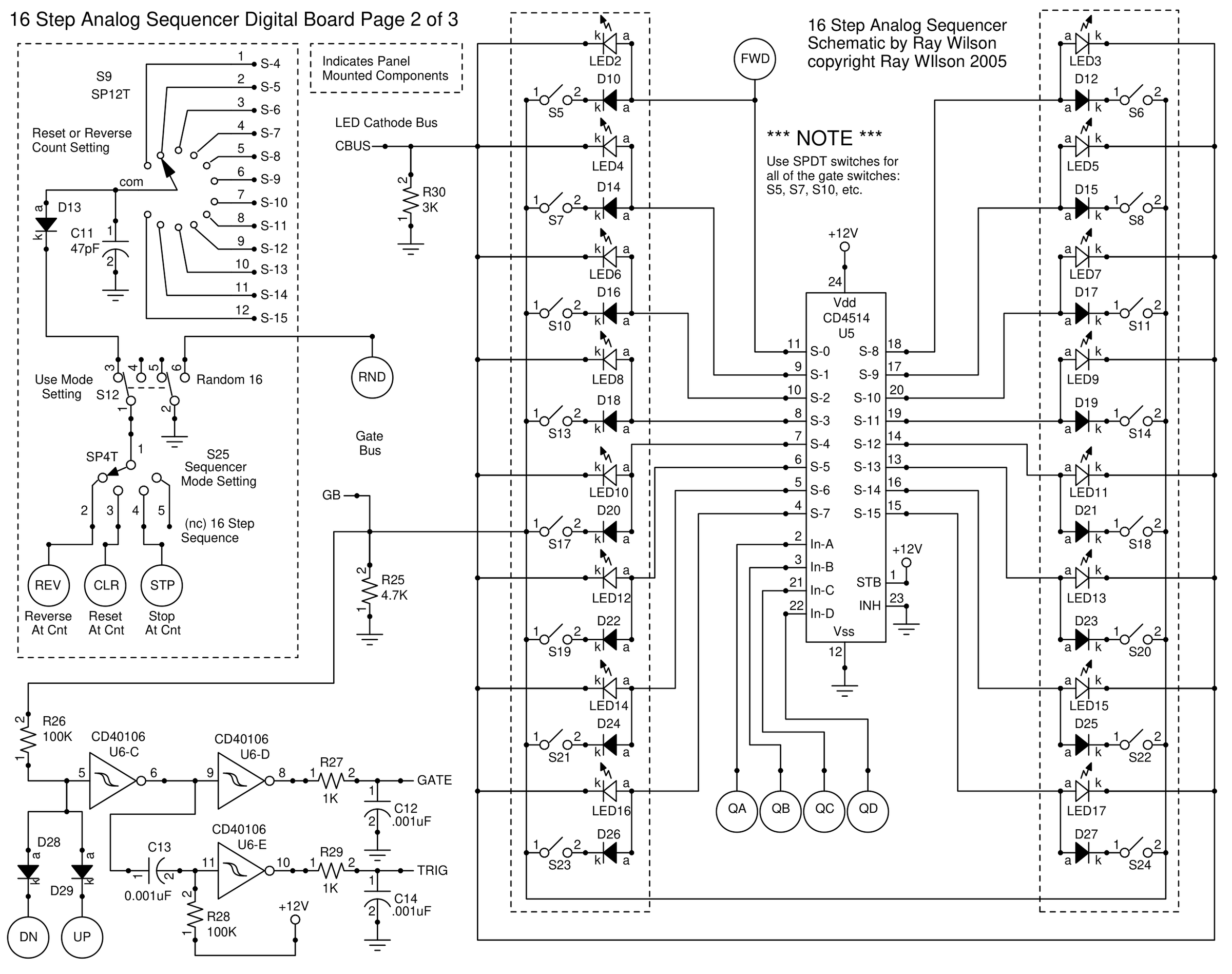
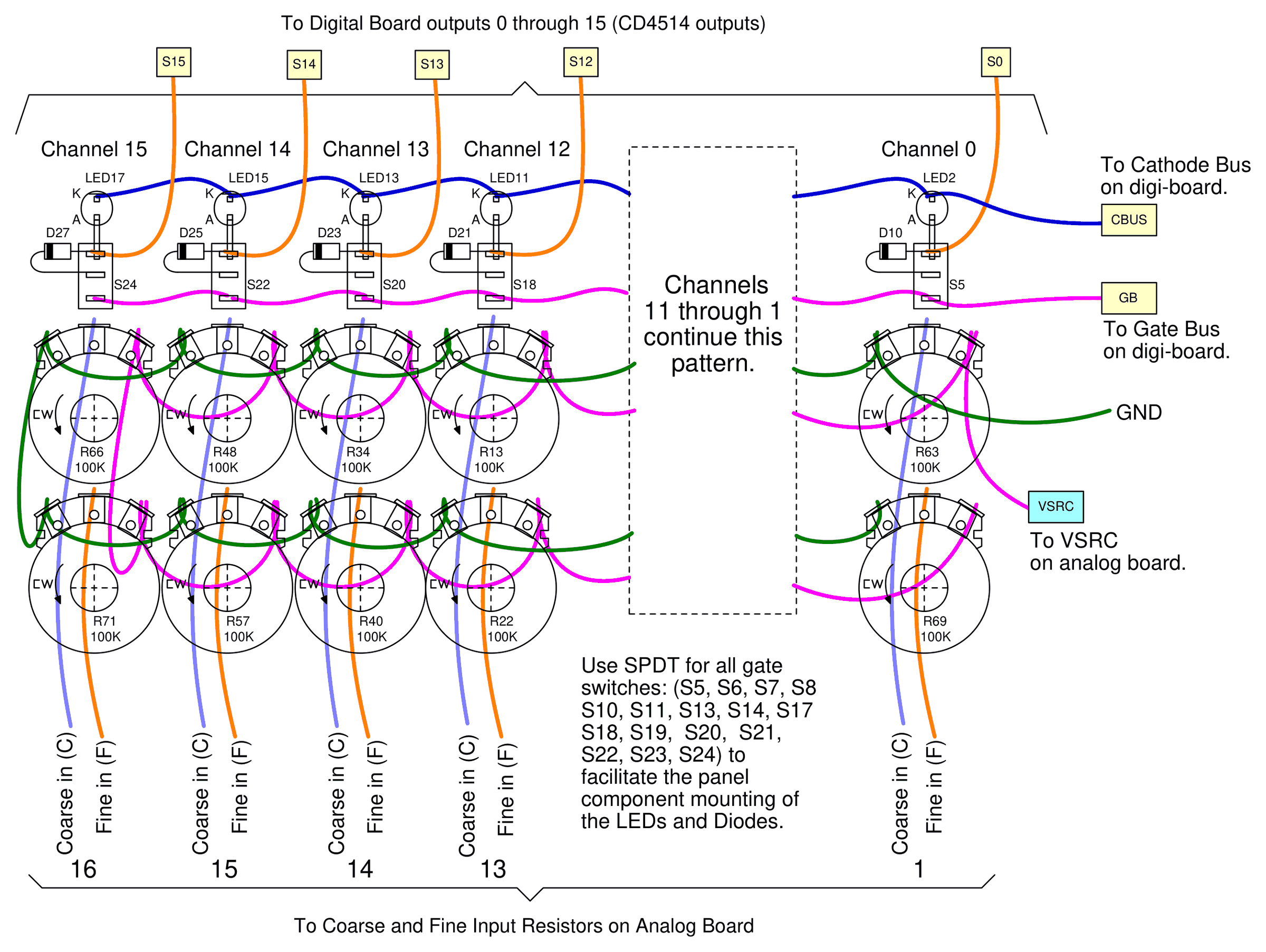
As explained above U5's 16 outputs go high corresponding to the current count (0 thru 15) on the outputs of U4 (QA thru QD). They are used to power the LED corresponding to the current step number. This LED lets you know which set of Coarse/Fine pots is the active one. Additionally each output (S0 thru S15) is fed to a switch and the anode of a diode which is used to control at which steps gate/trigger outputs are produced. Essentially the outputs of U5 are anded with the clock signal if the switch for a particular step is closed. I recommend using SPDT switches (even though the schematic shows SPST) to facilitate the panel wiring as shown in the panel wiring diagram. Note that both D13 and C11 are included in the panel wiring and are not shown on the PC board. All of the LEDs, switches and the diodes connected to the outputs of U5 are also part of the panel wiring.
Gate Bus (GB) is not shown on the PC board. Details of where to connect GB are explained below in the PC parts layout section.
Not Ray's words: that sentence came across from the 2005 page, where the first board had no GB hole. On this 2006 board the drawing under 16 Step Sequencer Board to Panel Wiring shows a pad labeled GB beside D30. Ray's 2005 workaround (tying the wire onto R25's lead) is on his previous version page.
16 Step Sequencer Schematic Page 3
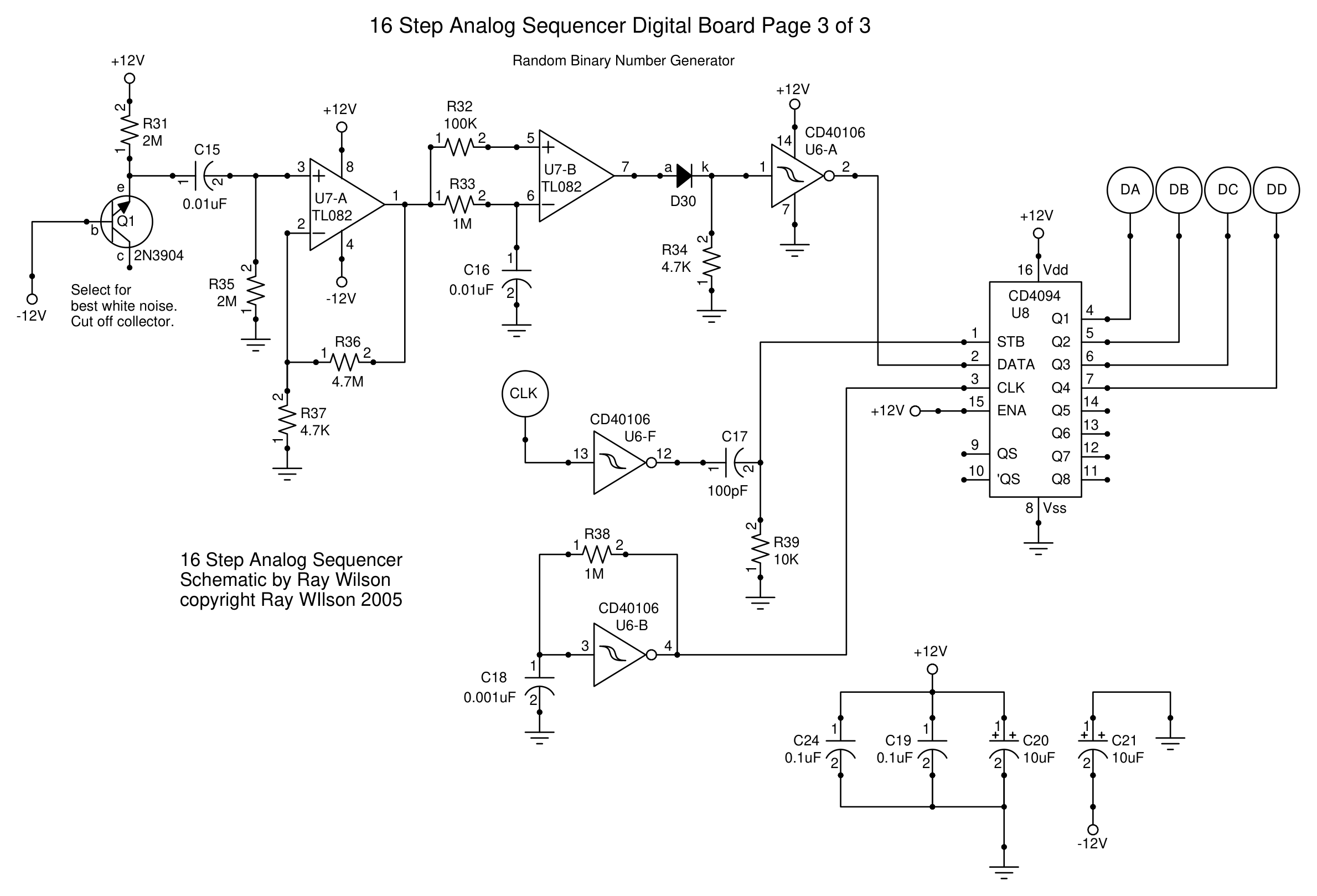
This is the simplest way I could come up with to generate random binary numbers. These are truly random because they are based on white noise and not any repeating pattern. Feel free to use this circuit in your super computer. Essentially, white noise is generated by Q1 and amplified to digital levels by the op amps and U6-A. This noise data is presented to the input of the shift register who is constantly clocked by the oscillating output of U6-B. Thus random ones and zeroes are constantly flowing through the shift registers internal flip flop chain. A positive pulse that corresponds to the low going edge of the clock signal is applied to the strobe input of the CD4094 which causes whatever number is floating through the shift register to be latched and presented to its outputs (DA through DD). These outputs are connected to the data inputs of U4. When U4's pin 11 is held low (Random 16 mode selected) U4 propogates the random 4 bit count to U5 on each main clock cycle and thus the 16 steps are randomly selected. Tune the steps to the scale of your choice and select random mode to hear a never repeating random melody.
16 Step Sequencer Panel Wiring
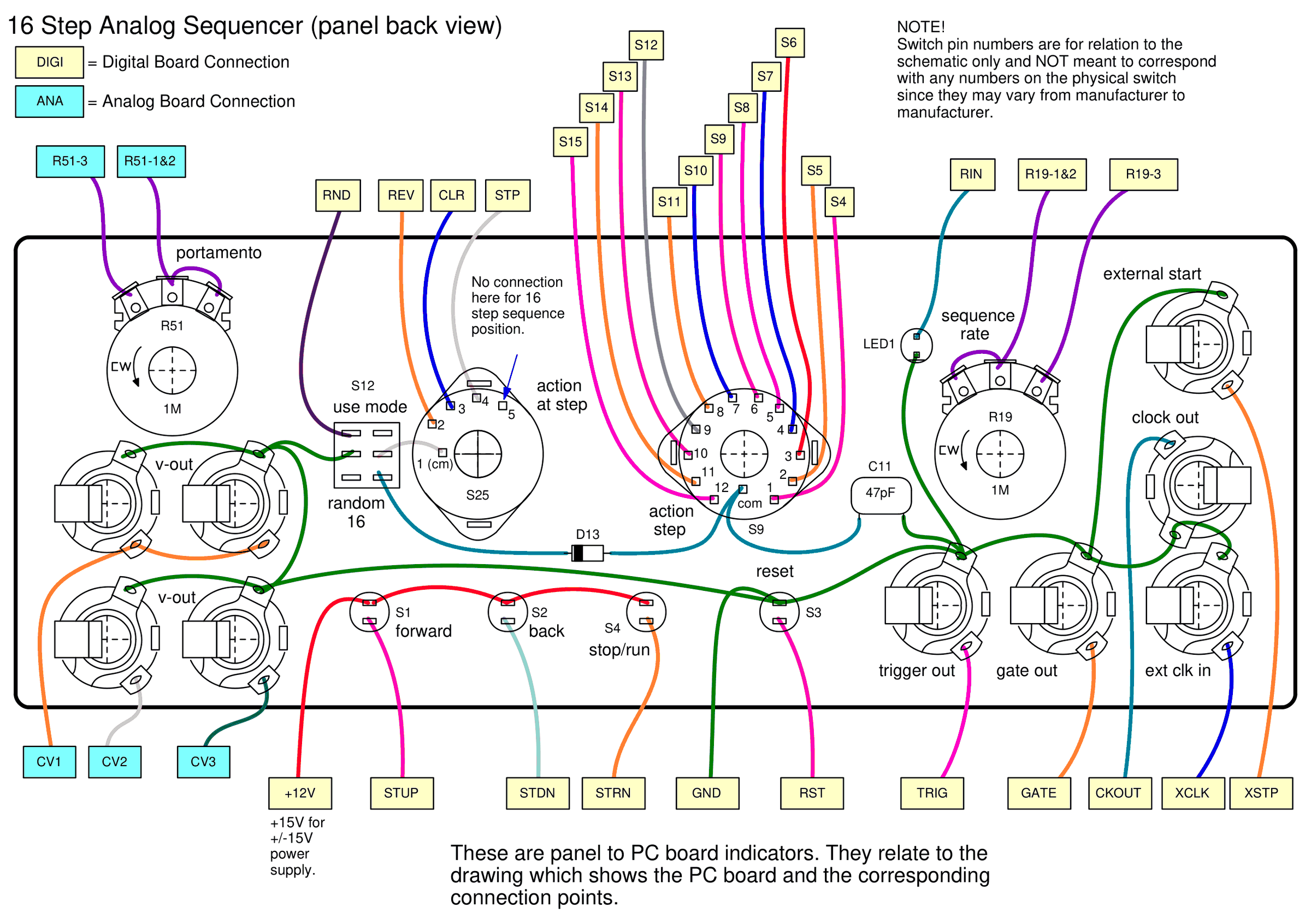
The control panel connections, read out as a list
tap to expand / collapse
Not Ray's words: the drawing above, read out tag by tag so a screen reader can reach it. The tag is the label on the board; the panel part is where that wire ends. Lug-level detail stays in the drawing.
| Board tag | Board | Goes to on the panel |
|---|---|---|
| CV1 | Analog | The upper pair of v-out jacks (the portamento outputs) |
| CV2 | Analog | Lower left v-out jack |
| CV3 | Analog | Lower right v-out jack |
| R51-3, R51-1&2 | Analog | Portamento pot R51, 1M |
| +12V | Digital | Forward S1, back S2 and stop/run S4 pushbuttons (+15V on a +/-15V supply) |
| STUP | Digital | Forward pushbutton S1 |
| STDN | Digital | Back pushbutton S2 |
| STRN | Digital | Stop/run pushbutton S4 |
| GND, RST | Digital | Reset pushbutton S3; GND also ties every jack sleeve together |
| RND | Digital | Use mode switch S12, the random 16 side |
| REV, CLR, STP | Digital | Action at step switch S25, lugs 2, 3 and 4; lug 5 has no connection (16 step); lug 1 goes to S12 |
| S4 through S15 | Digital | Action step switch S9, positions 1 through 12 in order; its common goes through D13 to S12 and through C11 47pF to ground |
| RIN | Digital | LED1, the clock rate indicator, other lead to ground |
| R19-1&2, R19-3 | Digital | Sequence rate pot R19, 1M |
| XSTP | Digital | External start jack |
| CKOUT | Digital | Clock out jack |
| XCLK | Digital | Ext clk in jack |
| TRIG | Digital | Trigger out jack |
| GATE | Digital | Gate out jack |
16 Step Sequencer Board to Panel Wiring
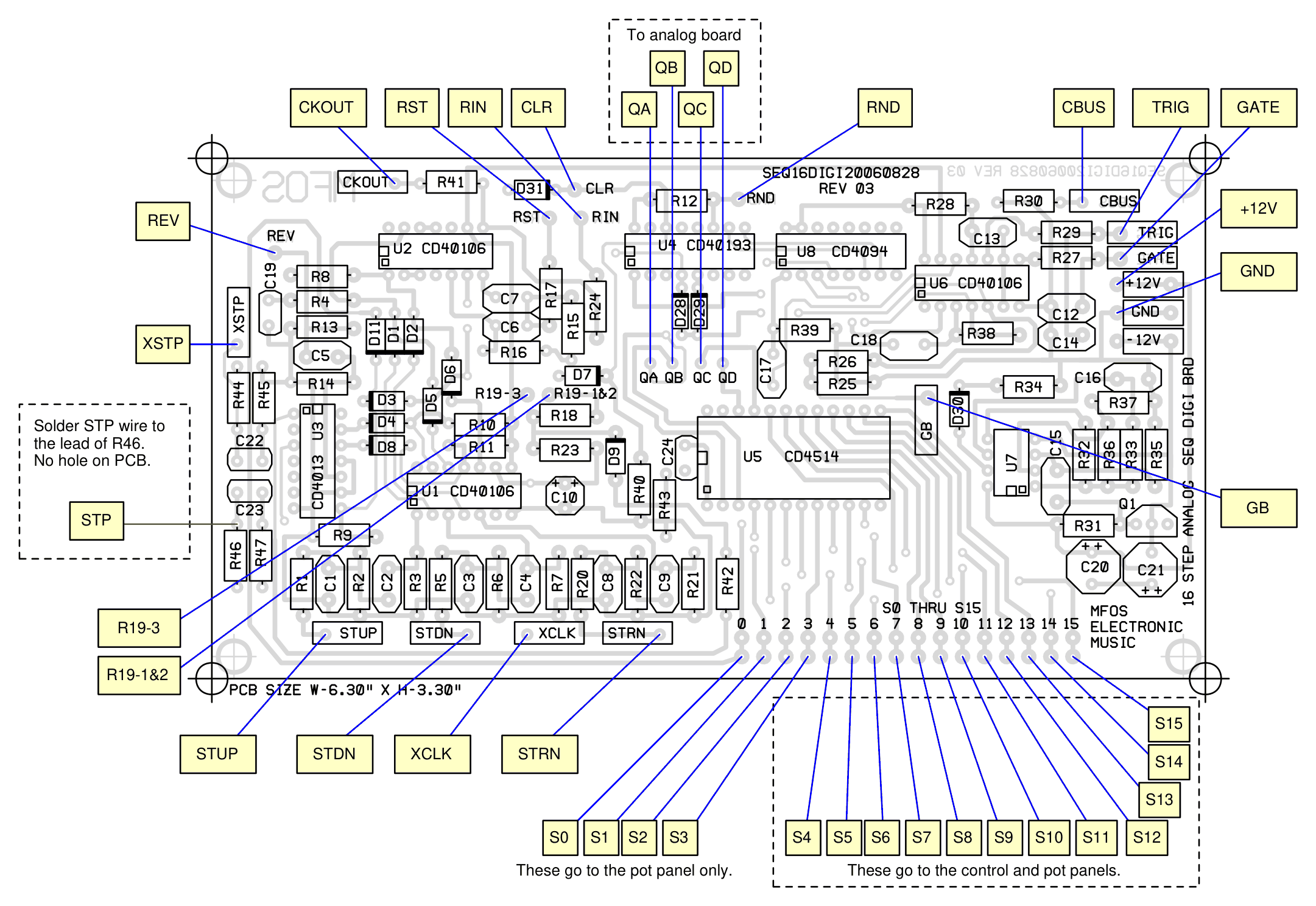
Digital board to panel wiring as PDF »
16 Step Sequencer Digital Board Parts List
| Qty. | Description | Value | Designators |
|---|---|---|---|
| 3 | CD40106(s) | CD40106 | U2, U1, U6 |
| 1 | CD4013 Dual D Flip Flop B | CD4013-B | U3 |
| 1 | CD40193 4 Counter | CD40193 | U4 |
| 1 | CD4094 8 Stage Shift/Store Reg | CD4094 | U8 |
| 1 | CD4514 4 Bit Latched 4 Dec. | CD4514 | U5 |
| 1 | TL082 Dual Op Amp | TL082 | U7 |
| 17 | LED(s) | General Purpose LED | LED1, LED5, LED3, LED9, LED7, LED13, LED11, LED17, LED15, LED4, LED2, LED8, LED6, LED12, LED10, LED16, LED14 |
| 31 | 1N914 Sw. Diode(s) | General purpose high speed switching diode | D2, D5, D6, D7, D1, D11, D3, D4, D8, D31, D9, D15, D12, D19, D17, D23, D21, D27, D25, D26, D24, D22, D20, D16, D18, D14, D10, D13, D28, D29, D30 |
| 1 | 2N3904 | 2N3904 | Q1 |
| 1 | Tantalum Capacitor | 1uF | C10 |
| 4 | Ceramic Capacitor(s) | .001uF | C14, C12, C13, C18 |
| 8 | Ceramic Capacitor(s) | .01uF | C22, C23, C1, C3, C8, C7, C15, C16 |
| 5 | Ceramic Capacitor | .022uF | C9, C2, C4, C5, C6 |
| 2 | Ceramic Capacitor(s) | .1uF | C19, C24 |
| 1 | Ceramic Capacitor | 100pF | C17 |
| 1 | Ceramic Capacitor | 47pF | C11 |
| 2 | Electrolytic Capacitor(s) | 10uF | C20, C21 |
| 1 | Linear Potentiometer | 1M | R19 |
| 8 | Resistor 1/4 Watt 5%(s) | 100K | R47, R9, R46, R44, R45, R28, R26, R32 |
| 7 | Resistor 1/4 Watt 5%(s) | 10K | R1, R5, R10, R11, R17, R20, R39 |
| 4 | Resistor 1/4 Watt 5%(s) | 1K | R42, R41, R29, R27 |
| 4 | Resistor 1/4 Watt 5%(s) | 1M | R13, R14, R33, R38 |
| 1 | Resistor 1/4 Watt 5% | 20K | R18 |
| 4 | Resistor 1/4 Watt 5%(s) | 220K | R7, R3, R16, R21 |
| 2 | Resistor 1/4 Watt 5%(s) | 2M | R31, R35 |
| 1 | Resistor 1/4 Watt 5% | 3.9K | R43 |
| 2 | Resistor 1/4 Watt 5%(s) | 3K | R24, R30 |
| 3 | Resistor 1/4 Watt 5%(s) | 4.7K | R25, R37, R34 |
| 1 | Resistor 1/4 Watt 5% | 4.7M | R36 |
| 4 | Resistor 1/4 Watt 5%(s) | 47K | R40, R12, R8, R4 |
| 1 | Resistor 1/4 Watt 5% | 6.2K | R23 |
| 4 | Resistor 1/4 Watt 5%(s) | 680K | R2, R6, R15, R22 |
| 1 | Single Pole 12 Throw Rotary Switch (non-shorting) | SP12T | S9 |
| 1 | Single Pole 4 Throw Rotary Switch (non-shorting) | SP4T | S25 |
| 1 | DPDT Switch | DPDT | S12 |
| 4 | SPST PB Switch(s) | SPST | S1, S2, S3, S4 |
| 16 | SPDT Switch (used to accomodate the gate diode and LED wiring) | SPDT | S5, S7, S10, S13, S17, S19, S21, S23, S6, S8, S11, S14, S18, S20, S22, S24 |
16 Step Sequencer Analog Board Information
16 Step Sequencer Analog Board Schematic
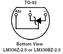
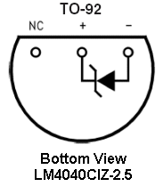
Either 2.5 Volt Reference chip will work.
Circuit Description
The analog section is driven by U4 (CD40193 Synchronous 4-Bit Up/Down Binary Counter) from the digital board. The 4 control lines QA, QB, QC, and QD determine which of the 16 inputs of the CD4067 (CMOS Single 16 Channel Multiplexer/Demultiplexer) is turned on to allow the voltage from the wipers of the channel's coarse/fine pot combination to be fed to the summing node (pin 2 of U3-A) via the channels mixing resistors (100K and 2M). U3-A acts as an inverting summer the output of which is fed to inverting unity gain buffer U3-B. U3-B's output is fed to the non-inverting inputs of voltage followers U1-D and U1-B whose outputs feed two of the CV output jacks of the sequencer.
U3-B's output also connects to one side of the Portamento pot R51 which provides an adjustable means to cause the voltage to slew from one channel's level to the next. As the pot is advanced the time to slew from one level to another (the time needed to charge and discharge C4 .1uF cap) is increased and visa versa. The output of U1-C feeds the CV output jack to which portamento can be applied (via setting of R51). Caps C2 and C3 are power supply bypass caps.
U1-A in conjunction with VS1 (LM336-2.5V 2.5 volt precision voltage reference) create a 7.5 volt source to which one side of all of the pots are connected. The precision voltage source applies a very clean 2.5V to the non-inverting input of U1-A. Feedback resistor R25 (200K) and gain set resistor R26 (100K) set the gain around U1-A to 3 which is how we get 7.5V from the 2.5V reference.
In operation when a digital count between 0 and 16 is applied to the QA-QD - AND ALL FINE POTS ARE AT 0 LEVEL - you should see the voltage present at the wiper of the channel's corresponding coarse pot at the output of U3-B plus or minus the op amp's offset voltage which should be a few millivolts. To test this on an isolated analog board (i.e. not connected to the outputs of U4) you can apply power supply levels (+12V and ground) to the QA through QD inputs to simulate the counts. Inputs connected to +12V simulate logic one level and inputs connected to ground simulate logic zero level. All QA through QD inputs must be connected or the test will not work. Floating CMOS logic levels tend to toggle from the slightest EM field. For example to simulate channel 0 being on connect QA through QD to ground. To simulate channel 5 being on ground QB and QD and apply +12V to QA and QC. You apply the binary code for the channel you want to test.
The CV output level for any channel should range from 0 to about 7.5V (coarse control turned up). The fine control will add 1/20 of the 7.5V range (.375V) to the output when at full level since it is entering summing inverter U3-A via a 2M resistor. Use 100K or higher pots for the controls since the parallel combination of all of the pots is the load seen by U1-A. With 100K pots U1-A is seeing about 3.125K which it is capable of driving. Lower value pots will cause the parallel combination of all of the adjustment pots to be too low and strain the operation of U1-A.
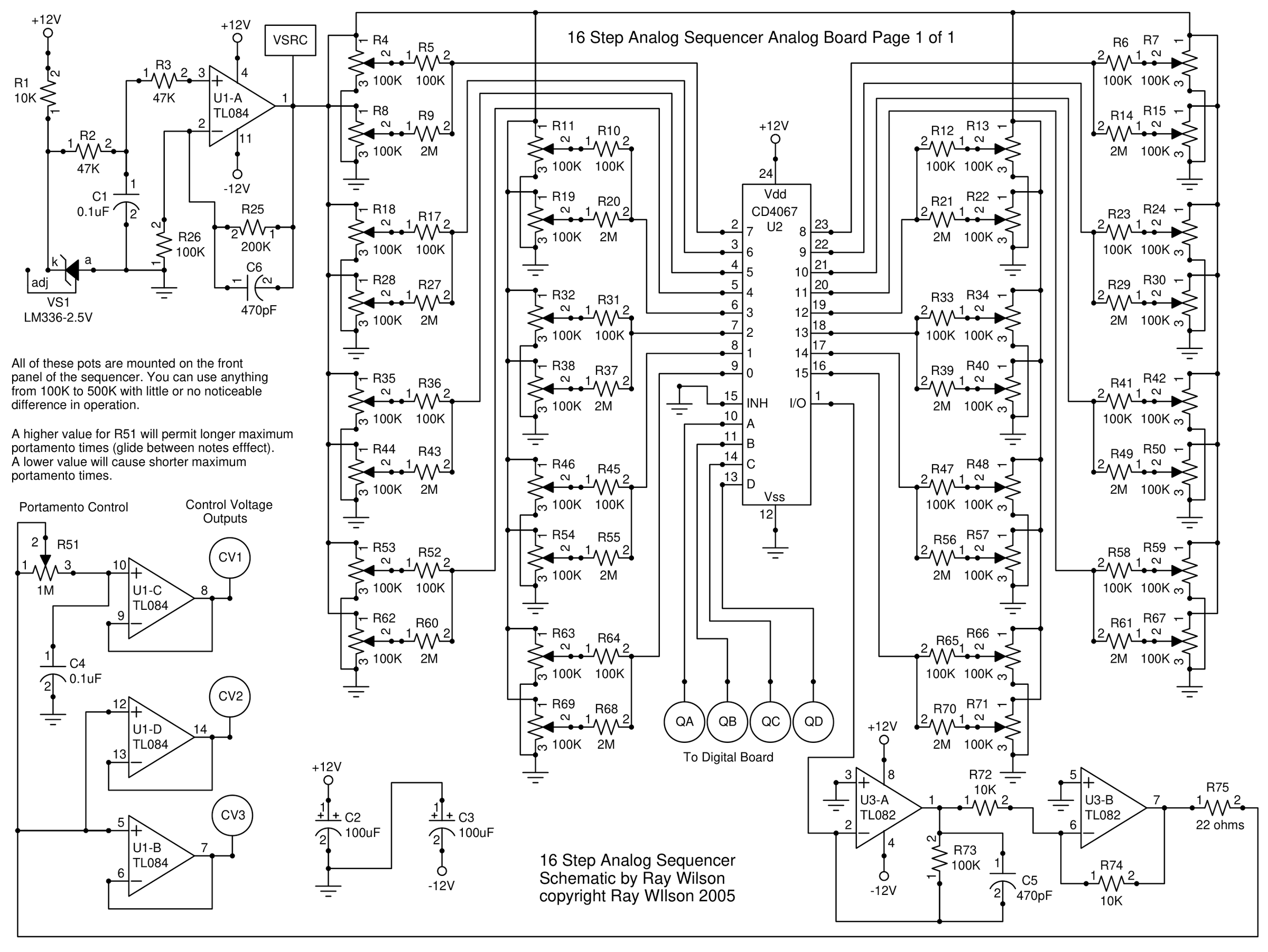
Analog board schematic as PDF »
16 Step Sequencer Panel Wiring Diagram
It is a good idea to mount the analog board near the voltage adjust pots. Remember that only the four digital contol lines need to be connected to the analog board from the digital board so they don't have to be mounted close together. There are a lot of wires between the analog voltage processor board and the pots so the closer they are to one another the better.
16 Step Sequencer Gate Switch Wiring Detail
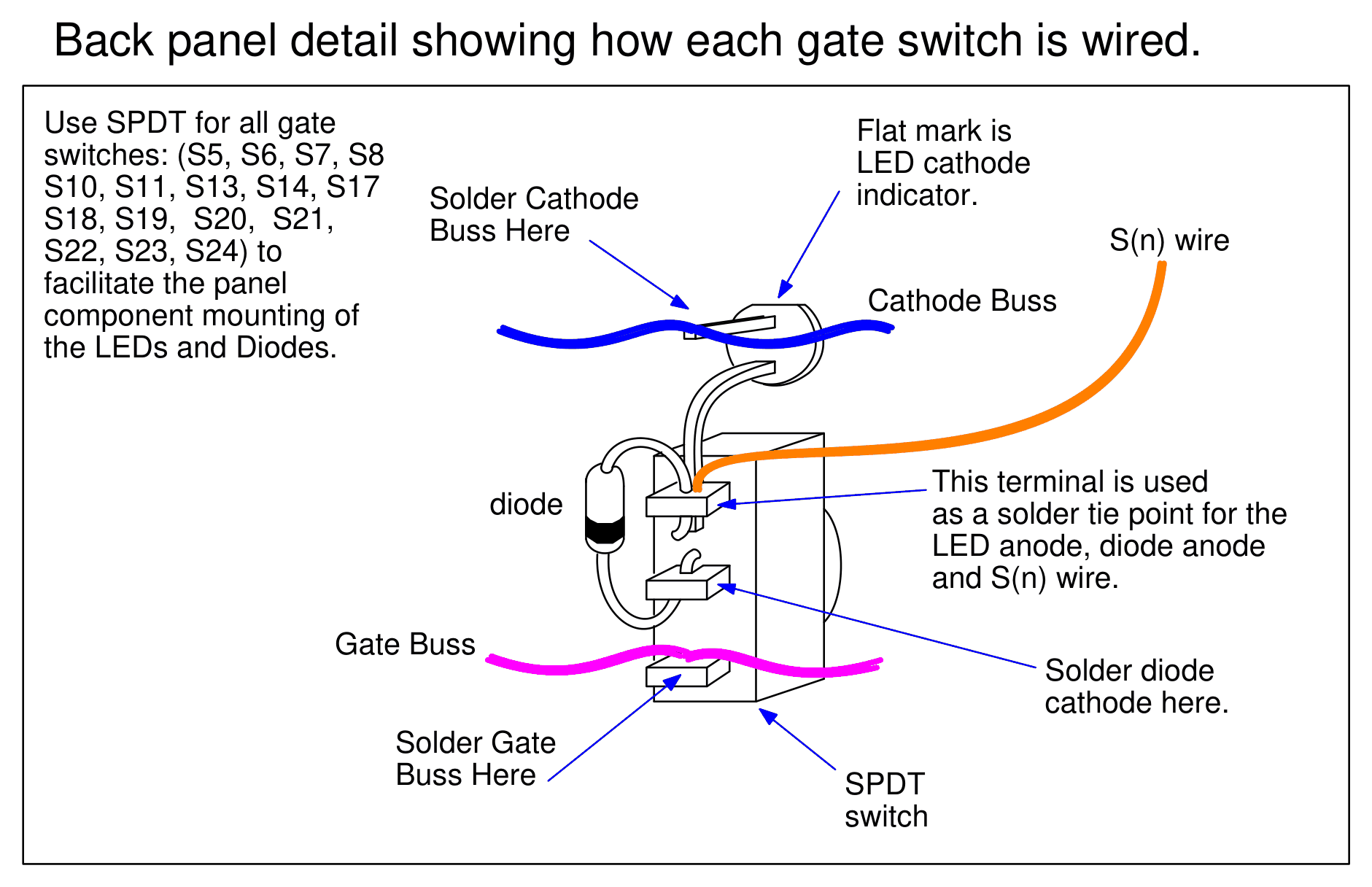
Gate switch wiring detail as PDF »
16 Step Sequencer Board to Panel Wiring Labels
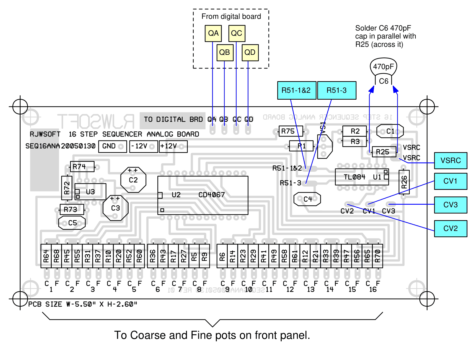
Analog board to panel wiring as PDF »
16 Step Sequencer Analog Board Analog Board Parts List
| Qty. | Description | Value | Designators |
|---|---|---|---|
| 1 | CD4067 Analog Mux/DeMux | CD4067 | U2 |
| 1 | TL082 Dual Op Amp | TL082 | U3 |
| 1 | TL084 Quad Op Amp | TL084 | U1 |
| 1 | LM336 2.5V Ref. | LM336-2.5V | VS1 |
| 32 | Linear Potentiometer(s) (don't forget to buy knobs) | 100K (up to 500K will work fine.) | R11, R19, R32, R38, R46, R54, R63, R69, R4, R8, R18, R35, R44, R53, R62, R13, R22, R40, R34, R48, R57, R71, R66, R7, R15, R30, R24, R42, R50, R67, R59, R28 |
| 1 | Linear Potentiometer | 1M | R51 |
| 18 | Resistor 1/4 Watt 1%(s) | 100K | R10, R31, R45, R17, R36, R12, R33, R47, R65, R6, R41, R58, R5, R52, R23, R64, R26, R73 |
| 3 | Resistor 1/4 Watt 1%(s) | 10K | R74, R72, R1 |
| 1 | Resistor 1/4 Watt 1% | 200K | R25 |
| 1 | Resistor 1/4 Watt 1% | 22 ohms | R75 |
| 16 | Resistor 1/4 Watt 1%(s) | 2M | R27, R20, R37, R68, R21, R39, R70, R14, R29, R49, R9, R60, R55, R61, R56, R43 |
| 2 | Resistor 1/4 Watt 1%(s) | 47K | R3, R2 |
| 2 | Ceramic Capacitor(s) | 0.1uF | C4, C1 |
| 2 | Ceramic Capacitor(s) | 470pF | C6, C5 |
| 2 | Electrolytic Capacitor(s) | 100uF | C3, C2 |
Parts Layouts
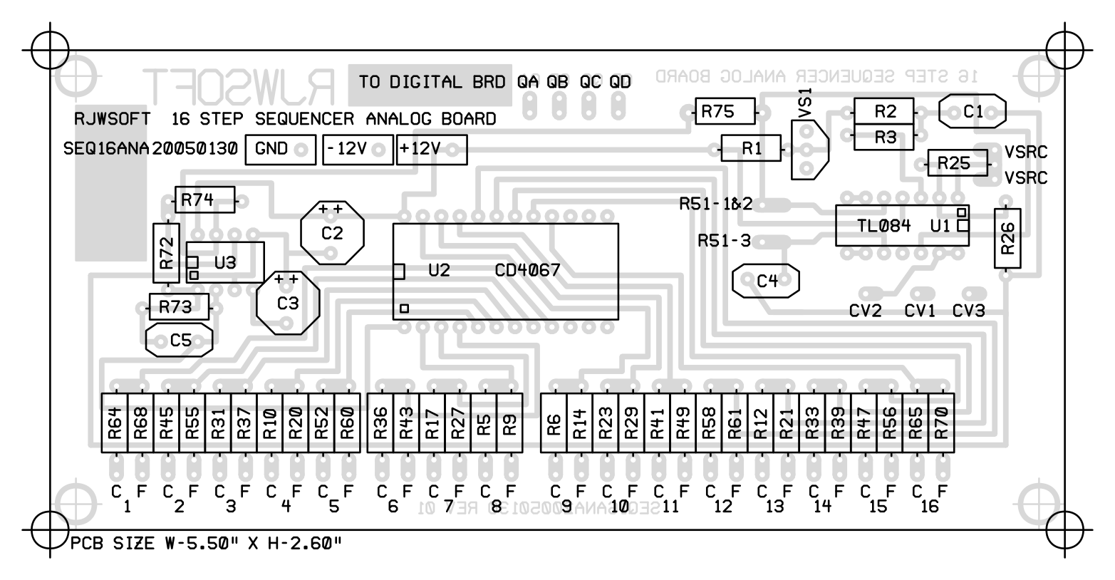
Analog board parts layout as PDF »
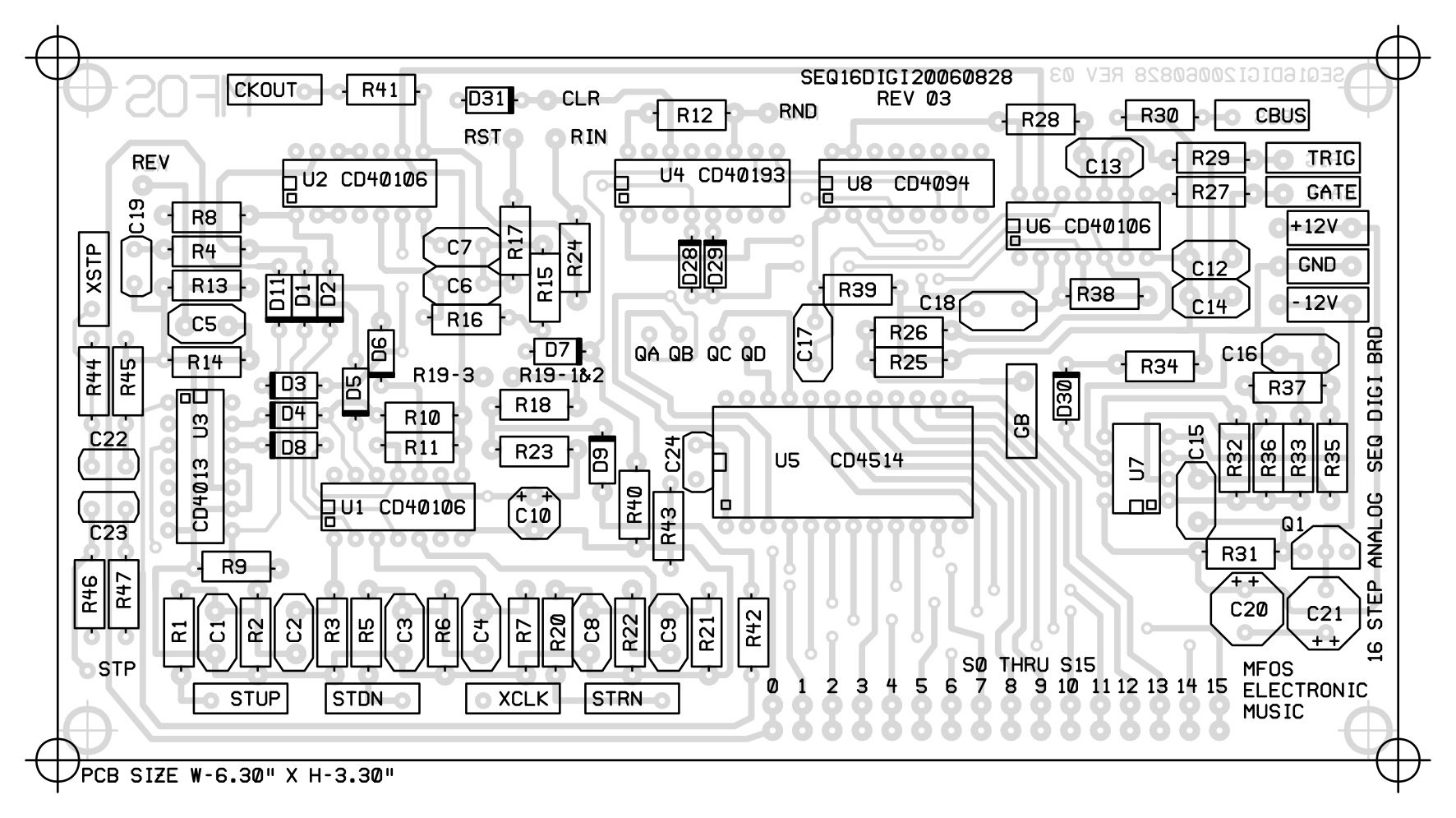
Digital board parts layout as PDF »
Panel Overlays
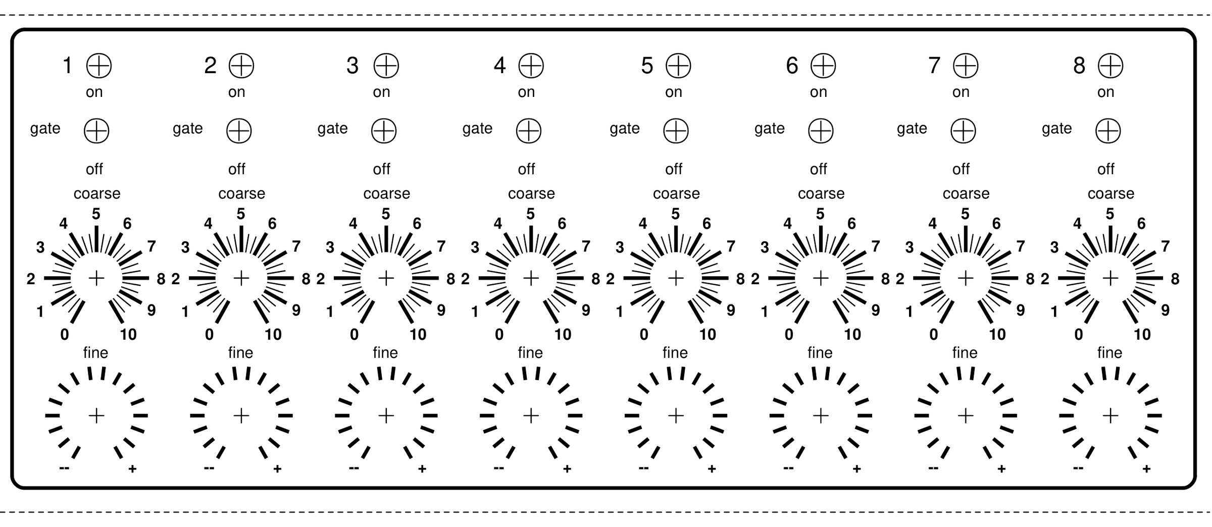
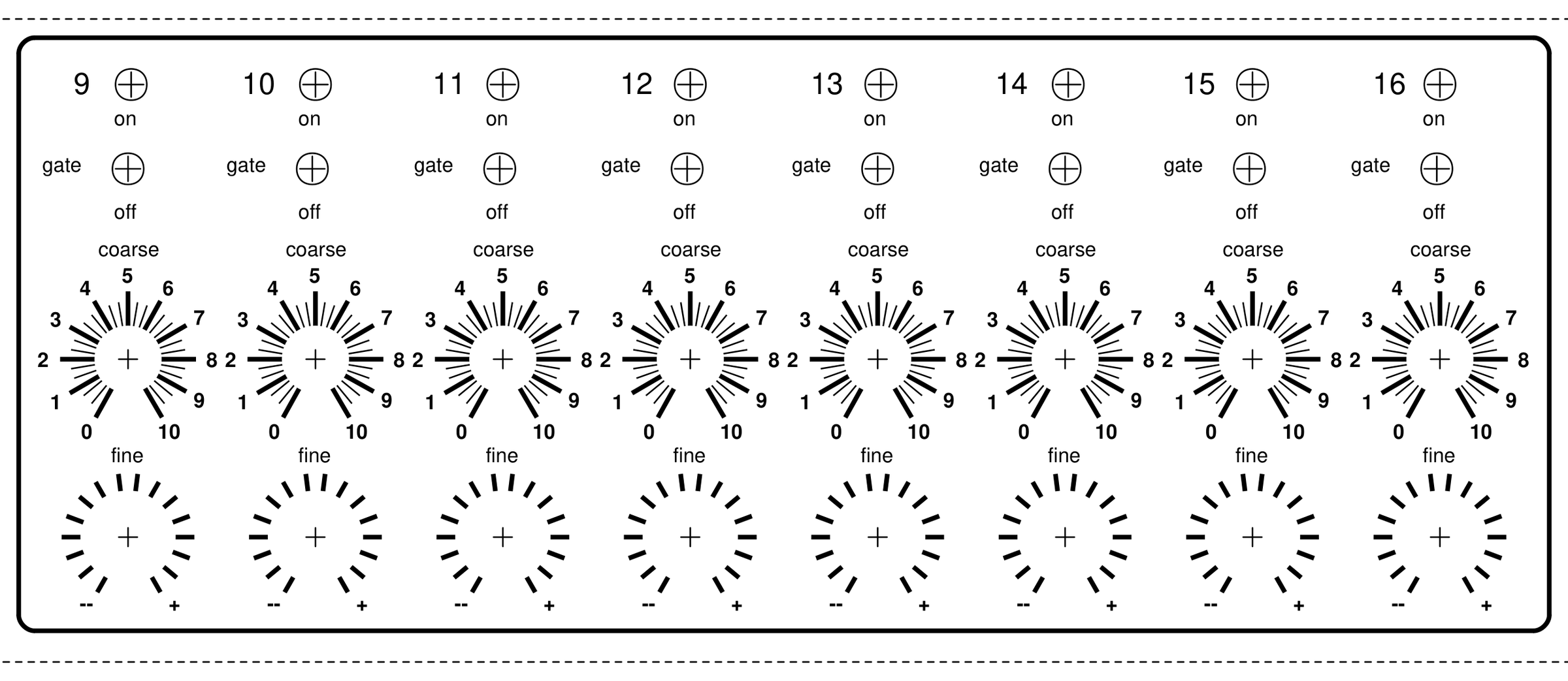
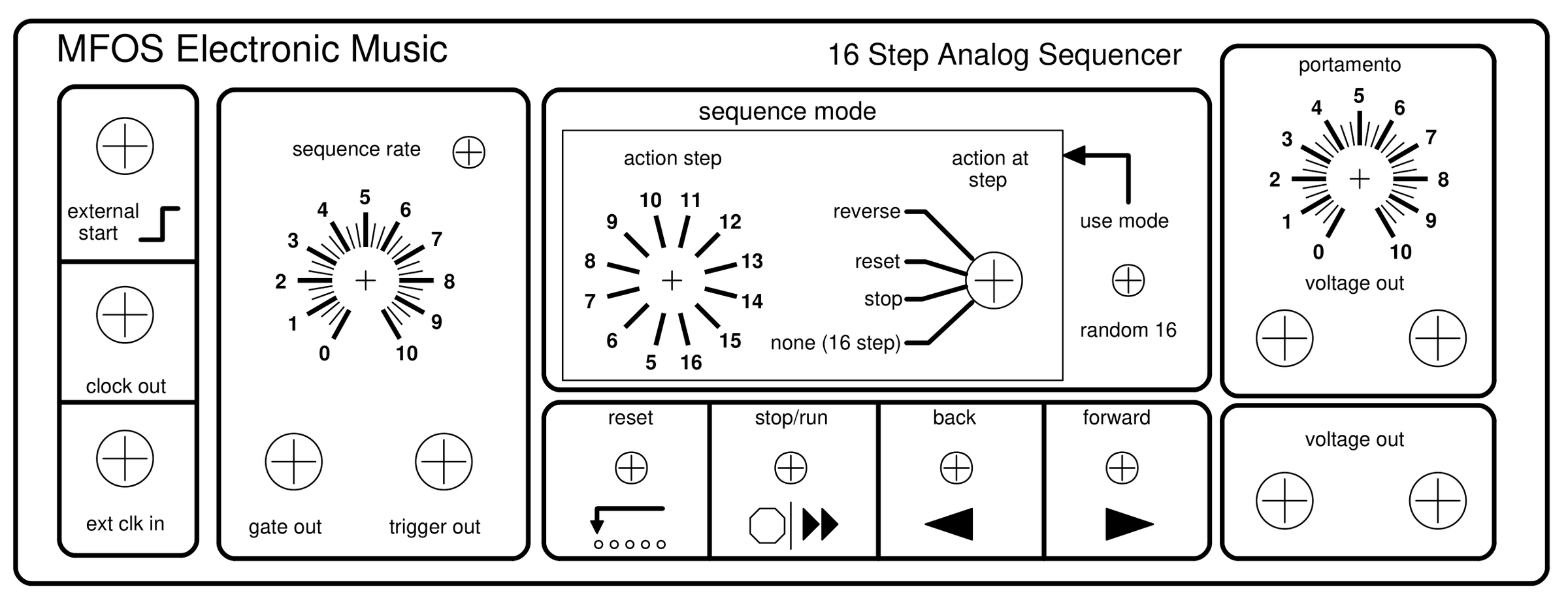
Panel Overlay contributed by Jeff Johnson of Texas
This is a cool one piece template. I suggest you sketch a corresponding wiring diagram for it to avoid wiring errors during construction if you go with this template design.
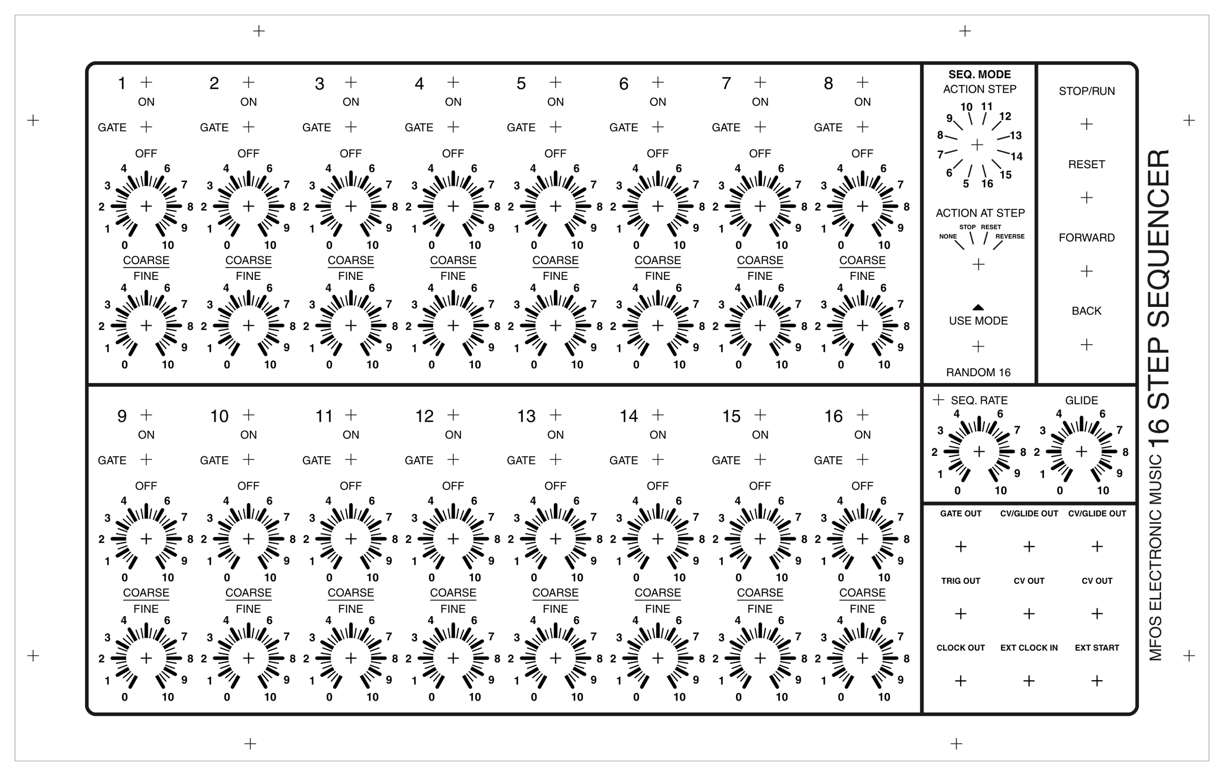
Jeff Johnson's template as PDF »
Panel Overlay contributed by John Ibbotson of the United Kingdom
This is a cool one piece template. I suggest you sketch a corresponding wiring diagram for it to avoid wiring errors during construction if you go with this template design. This file is for use with Front Panel Designer.
John Ibbotson's panel as a Front Panel Designer file »
PCB Images X2 Artwork GIF files
By the time you've etched (double sided by the way) and drilled (587 holes) these boards yourself you'll wonder why you didn't buy the professionally manufactured, glass epoxy, plated through-hole, double sided, soldermasked, silk screened legend board from me. But have at it... These X2 images are provided for individual use and not for mass production or sale.
Miscellaneous
- 1/16" to 1/10" Thick aluminum plates for mounting the pots and switches.
- Wood or plastic to build a case with.
- Assorted hardware 1" 6-32 nuts and bolts, 1/2" #8 wood screws, etc
- Knobs for potentiometers, wire and solder.
- Digital Volt Meter and a Signal Tracer or oscilloscope for testing.
Adding More Analog Sequencer PCBs
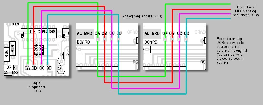
"Daisy Chaining" more Analog PCBs
You can drive more than one analog sequencer board from one digital board. This is accomplished by chaining the QA, QB, QC, and QD connections from the digital sequencer board to one or more additional analog sequencer boards. The illustration below shows this. Each additional analog PCB requires it's own set of coarse and fine pots and a new set of CV output jacks and portamento control. These are mounted on a panel and wired just like the original set of coarse/fine pots, CV out jacks and portamento pot.
The result is that you can now control separate modules with a synchronized 16 step sequence. You still only get 16 steps. Adding analog PCBs does not result in more steps. Adding more analog boards lets you do things like: have a 16 step sequence of chords (controlling separate VCOs) or control a VCF with one set of controls and some oscillators with the other set. You can imagine a ton of cool applications.
How should I drive additional channel indicator LEDs?
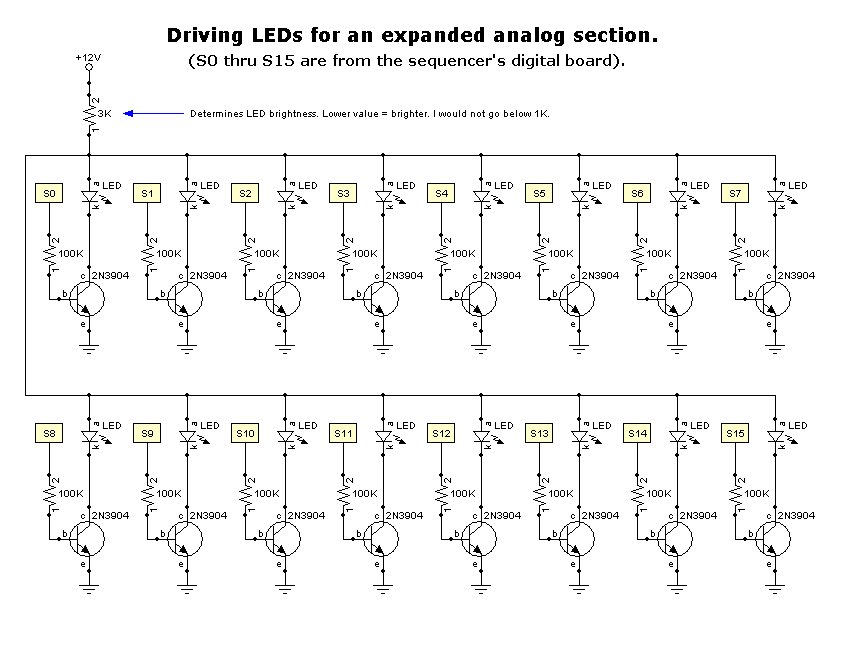
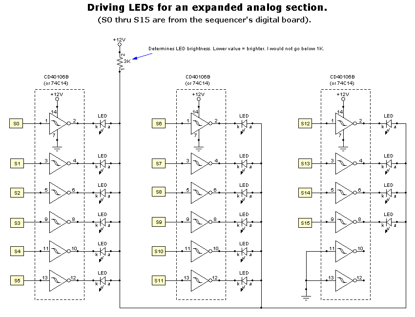
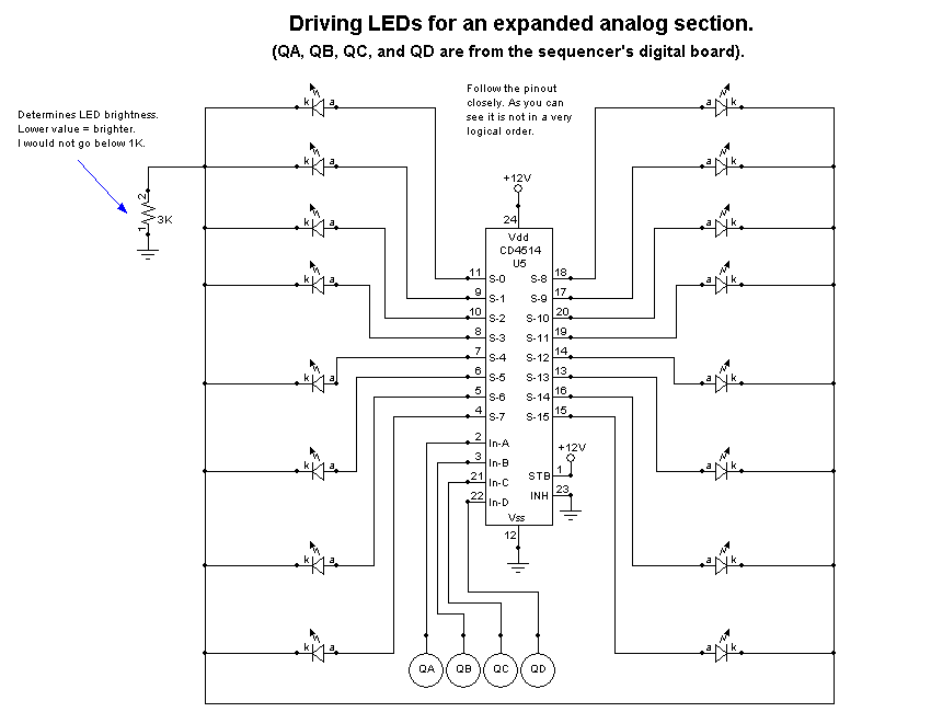
Although you can probably get away with another set of LEDs being driven in parallel with the original ones I recommend that you isolate the original driving circuit and add buffers of one kind or another to each set of new LEDs. Below I show three different ways to drive an expanded analog section's indicator LEDs. One way uses NPN transistors as buffers another way uses hex inverting Schmitt triggers (CD40106) and finally a single chip solution is to use a CD4514 (CMOS 4-Bit Latch/4-to-16 Line Decoder). Either will work fine and either can be built on a small daughter board. The choice of which to use may be as simple as what's in your parts cabinet currently, trannies, inverters or a spare CD4514.
Here, transistors are used to drive the LEDs. The original S0 through S15 circuit points can be accessed at the digital board by carefully tack soldering the new wires to the bottom of the board or at the panel where they connect to the gate switches and LEDs. A successfully tack soldered joint should look nice and shiny (like any other solder joint). If your tacked connection turns out clumpy then use some fluxed braid to remove the excess and try again.
Here I show you how to use inverting buffers to drive the LEDs. This method uses way less parts and is probably my favorite. Either of these methods should fit nicely on a small daughter board.
Lastly this is the CD4514 method. It uses one chip and notice that the QA thru QD inputs are used to drive it. These come from the analog board and will most likely need to be tack soldered to the bottom the QA thru QD pads on the board.
All work © Ray Wilson / Music From Outer Space - musicfromouterspace.com. The 16 Step Sequencer, its circuit, text and drawings are Ray's. The rotary sequencer photo is Thomas White's, and the two one-piece panels are Jeff Johnson's and John Ibbotson's, as shared on Ray's page.
Mirrored and recoded by Mess O' Pedals to preserve Ray's work and keep it accessible. Only the HTML is mine - the design, the words, and the wit are all Ray Wilson's.