Envelope Follower
Audio in, CV out · One LM324 on thirteen strips · By Onion Madder · Mess O' Pedals
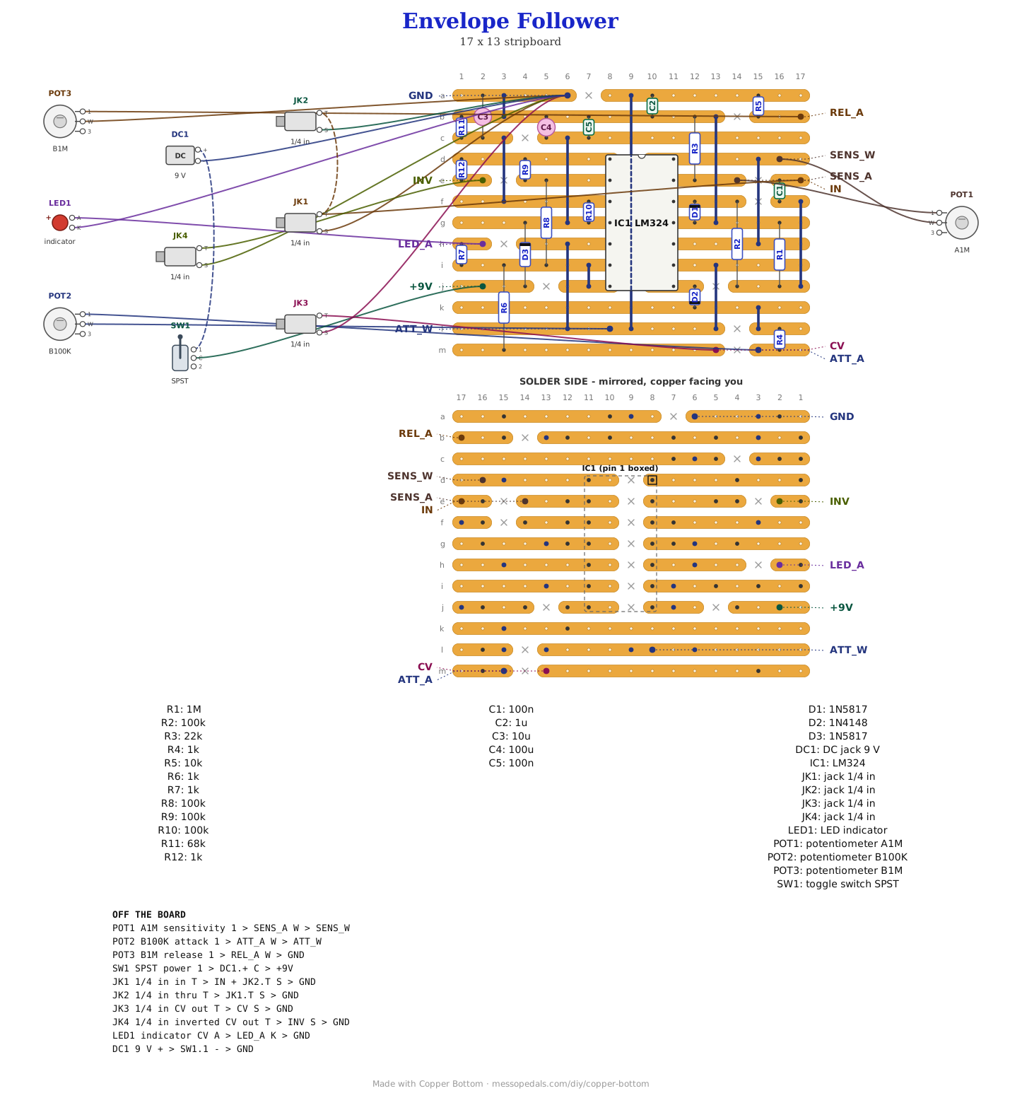
Plug a guitar, a drum machine or a synth into it and the CV jack gives back a voltage that follows how loud it is: up when you hit a note, down as it fades. A second jack gives the same thing upside down, high in silence and dropping as the sound gets louder. Three knobs: sensitivity for how hard it listens, attack for how fast it rises, release for how slowly it lets go. A THRU jack passes the sound on untouched, and an LED shows the CV. One chip on a 13 by 17 board, from 9 V, ready to push the Opto Duet CV around.
What you'll need
tap to expand / collapse
- 1× LM324 quad op-amp, 14-pin DIP (IC1) - spot it: LM324 printed on top, a notch or a dot at pin 1. It has to be a single-supply op-amp whose inputs work down to 0 V: an LM324 or LM2902 sits in the same holes. A TL074 will not work from one 9 V supply
- 2× 1N5817 Schottky diode (D1, D3) - spot it: a fat black body with a gray band. D3 stands in the supply against a reversed plug; D1 stands between the ground pin and pin 12 and keeps the input from being dragged below ground
- 1× 1N4148 diode (D2) - spot it: a little glass bead with a black band. The peak catcher's diode
- 4× 100K resistor (R2, R8, R9, R10) - spot it: bands brown-black-yellow
- 4× 1K resistor (R4, R6, R7, R12) - spot it: brown-black-red
- 1× 1M resistor (R1) - spot it: brown-black-green
- 1× 68K resistor (R11) - spot it: blue-gray-orange
- 1× 22K resistor (R3) - spot it: red-red-orange. With the sensitivity pot it sets the gain
- 1× 10K resistor (R5) - spot it: brown-black-orange. The shortest release the knob can reach
- 1× 1 µF film capacitor (C2) - spot it: a small box marked 105. The hold cap. Film, not an electrolytic: an electrolytic leaks, and the leak would be a second release knob you cannot turn
- 1× 100n film capacitor (C1) - spot it: a small box marked 104. The input cap
- 1× 100n ceramic (C5) - spot it: 104. Across the supply
- 1× 100 µF electrolytic (C4) and 1× 10 µF electrolytic (C3) - spot it: a can with a stripe down the negative side
- Stripboard, 13 strips × 17 holes or larger, and solid wire for eleven links. One runs under the chip, down the column of cuts in the middle, so lay it before the chip goes in
Off the board
- 1× A1M pot, SENSITIVITY - spot it: A1M or 105A on the back. Wired as a variable resistor: lug 1 and the wiper, lug 3 empty
- 1× B100K pot, ATTACK - B104 on the back. Lug 1 and the wiper
- 1× B1M pot, RELEASE - B105 on the back. Lug 1 to REL_A, the wiper to ground
- 4× 1/4 in mono jacks: IN, THRU, CV OUT and INV OUT
- 1× LED, any color - it shows the CV
- 1× 9V DC jack, or a 9V battery and snap
- 1× SPST toggle, the power switch, in the positive lead between the supply and the +9V pad
The layout file is the guide
Like the rest of the stripboard shelf, the build document for this one is the file itself: ↓ Download Envelope_Follower.json - import it into Copper Bottom and the editor gives you the board picture, the placement walkthrough, the electrical checks and a printable build sheet, all from the same file. No coordinates are written out on this page on purpose: the editor is the viewer, and a number typed twice is a number that can drift.
The netlist
Quoted verbatim from the layout file. It says what each strip is supposed to be doing while you stare at it, and it carries the circuit somewhere else if you want to lay it out your own way.
The off-board wiring
Eleven pads leave the board. In on the left of the box, outs on the right.
| Pad | Goes to |
|---|---|
| +9V | The power switch; the switch's other side to the DC jack's center pin, or the battery snap's red lead |
| GND | The DC jack's sleeve or the battery's black lead, every jack sleeve, the LED's cathode and the RELEASE pot's wiper |
| IN | The IN jack's tip. The THRU jack's tip is wired straight across to it |
| SENS_A, SENS_W | The SENSITIVITY pot: lug 1 and the wiper. Turned down it is x1, up about x46 |
| ATT_A, ATT_W | The ATTACK pot: lug 1 and the wiper |
| REL_A | The RELEASE pot's lug 1; its wiper goes to GND |
| CV | The CV OUT jack's tip |
| INV | The INV OUT jack's tip |
| LED_A | The LED's anode, the long leg |
How it works, in one breath
Four op-amps in one chip, one job each. The first is a gain stage: the sensitivity knob takes it from x1 to about x46, and because the chip runs from one 9 V supply, the negative halves of the sound simply flatten at 0 V, which turns the audio into a row of positive bumps. The second catches the top of each bump: it charges C2 through a diode and the attack knob, and because the diode sits inside its loop, the CV starts from 0 V instead of 0.6 V up. C2 drains through the release knob, so the CV holds the last peak and lets go slowly. The third is a buffer, so the jack and the LED never pull on C2. The fourth flips the CV around a reference of about 3.5 V, so the inverted jack sits at about 7 V in silence and falls as the other one rises. By the arithmetic, attack runs from about 1 to 100 ms, release from about 10 ms to a second, and the CV from 0 to about 7 V.
Things to try
- Into the Opto Duet CV. CV OUT into the pitch jack and the voice rises with every note you play into it; INV OUT into the tempo jack and loud passages speed the engine up
- A longer release. C2 at 2.2 µF doubles every time on both knobs. Keep it film
- Drums. Attack all the way down and release short, and every hit becomes a gate-shaped pulse
- Into a rack. The Follower Rack is the same circuit on a TL074 and ±12 V, with the same three knobs
The circuit is the textbook envelope follower - a gain stage, a peak detector with its diode inside the loop, a buffer - with an inverter added for the second out. The layout is Onion Madder's, drawn in Copper Bottom.