Utility LFO
Triangle, square and sine, one knob for speed and one for how much · By Onion Madder · Mess O' Pedals
A low-frequency oscillator is a knob that turns itself. This one makes three shapes at once - a triangle, a square and a sine - picks one with two toggles, and puts it out through a LEVEL knob as a control voltage that sits on the half rail, so it drives the CV input of any 9 V box on this site straight: the Dragonfly's CV in, a 555's pin 5, the far side of a vactrol. A RANGE toggle makes it ten times slower, and an LED blinks the rate. One TL074 does all of it; the Dual-Wave LFO on this shelf is the same core with half the chip and a blend knob instead of a switch.
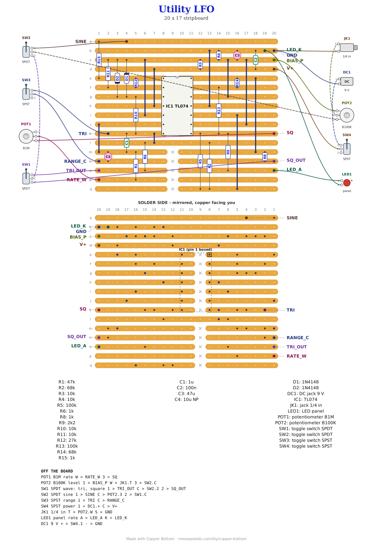
What you'll need
tap to expand / collapse
Twenty-nine parts on the board, counting the links, and nine off it. Nothing exotic: one quad op-amp and a bag of resistors.
- 1× TL074 quad op-amp, DIP-14 (IC1) - spot it: fourteen legs, TL074 printed on top, a notch at one end. A TL084 or an LM324 sits in the same holes; the LM324 swings closer to ground but is slower on the corners of the square. Fit a socket
- 2× 100K resistor (R5, R13) - spot it: bands brown-black-yellow. R5 is the comparator's feedback, the one that sets the window; R13 feeds the square into its scaler
- 2× 68K resistor (R2, R14) - spot it: bands blue-gray-orange. R2 takes the triangle to the comparator, R14 is the scaler's feedback. Do not swap R2 and R5: 68K on the triangle side and 100K on the feedback side is what makes the trigger window narrower than the swing. The other way round it never starts
- 1× 47K resistor (R1) - spot it: bands yellow-violet-orange. The floor under the RATE pot: with the knob at zero this is all the resistance the integrator has, so it sets the fast end
- 1× 27K resistor (R12) - spot it: bands red-violet-orange. The sine stage's feedback: 27K over R11's 10K is a gain of 3.7, which lands the rounded triangle at the same height as the other two waves
- 4× 10K resistor (R3, R4, R10, R11) - spot it: bands brown-black-orange. R3 and R4 make the half rail - a matched pair is nice, not necessary. R10 feeds the triangle into the sine diodes and is the one to change if the sine looks wrong; R11 is the sine stage's other leg
- 1× 2K2 resistor (R9) - spot it: bands red-red-red. The LED's series resistor, off the raw square
- 3× 1K resistor (R6, R8, R15) - spot it: bands brown-black-red. One in each output, so a shorted lead costs nothing
- 2× 1N4148 (D1, D2) - spot it: tiny glass body, black band toward the cathode. Back to back between the sine node and the half rail: they are the sine shaper, and the whole of it
- 1× 1 µF film (C1) - spot it: a small box, printed 105. This is the timing cap, between the integrator's input and its output. Film, not electrolytic: it swings both ways around the half rail
- 1× 10 µF bipolar electrolytic (C4) - spot it: a can marked NP or BP, no stripe. The RANGE cap; it swings both ways too, which is why it cannot be an ordinary polarized one. Two 22 µF polarized cans back to back, minus to minus, are the same thing if you have no bipolar
- 1× 47 µF electrolytic (C3) - holds the half rail still. Stripe to ground
- 1× 100nF ceramic (C2) - spot it: printed 104. Supply decoupling, beside the chip's pin 4
- 9× wire links (J1 to J9) - offcuts of component leg. Every op-amp pin the panel needs is carried to a strip of its own by one of these, because a chip pin's strip has two neighbors and both are other pins
- 1× DIP-14 socket
Off the board
- 1× B1M linear pot - RATE. Wired as a variable resistor: lug 3 to SQ, the wiper to RATE_W, lug 1 left empty. The 47K floor it needs is already on the board
- 1× B100K linear pot - LEVEL. Wired as a divider: lug 1 to BIAS_P, lug 3 to the sine toggle's common, the wiper to the output jack tip. Turned all the way down the output sits on the half rail, not ground
- 2× SPDT toggle, on-on - the wave pick. WAVE: lug 1 to TRI_OUT, lug 2 to SQ_OUT, common to the SINE toggle's lug 2. SINE: lug 1 to SINE, lug 2 from the WAVE toggle's common, its own common to the LEVEL pot's lug 3. Two toggles because an on-off-on has nothing in the middle
- 1× SPST toggle - RANGE, between TRI and RANGE_C. Closed, C4 sits across C1 and everything is ten times slower
- 1× LED - long leg to LED_A, short leg to LED_K. R9 is on the board, so nothing else goes with it
- 1× 1/4″ jack - the output. Tip from the LEVEL wiper, sleeve to GND. A 3.5 mm jack if the box it feeds has one
- 1× DC jack, 9 V, or a battery snap. 12 V is fine and gives every wave a little more swing
- An SPST toggle for power, in the positive supply lead between the DC jack or battery and the board's V+ pad. Not in the layout file - it is off the board, and every build on this shelf gets one
The layout file is the guide
Like every layout on this shelf, the build document for this one is the file itself: ↓ Download Utility_LFO.json - import it into Copper Bottom and the editor gives you the board picture, the placement walkthrough, the electrical checks and a printable build sheet, all from the same file. No coordinates are written out on this page on purpose: the editor is the viewer, and a number typed twice is a number that can drift.
Three rails, one strip each. Strips b, c and d are ground, the half rail and V+, straight above the chip, and every reference on the board is the half rail - the chip's pins 5, 9 and 12 all link up to strip c. The columns under the chip carry nothing but the cut. Below the chip, strip l carries the triangle across the board, and the five strips under that are cut in two at column 9 so each half is a net of its own.
The netlist
Quoted verbatim from the layout file, and emitted from the copper rather than typed
beside it - so checking the board against it can only pass. What it is for is carrying the
circuit somewhere else, and telling you what each strip is doing while you stare at it. The
four nets that matter are TRI, SQ, IC1_INC (the
comparator's trigger point, where R2 and R5 meet) and IC1_INA_2 (the sine
node, where the diodes live).
The off-board wiring
Twelve pads leave the board: two knobs, three toggles, a jack, an LED and the supply.
| Pad | Goes to |
|---|---|
| SQ / RATE_W | The RATE pot, a variable resistor: lug 3 to SQ (the raw square, about 1 to 8 V), wiper to RATE_W, lug 1 empty. Same shape as the Dual-Wave's rate knob |
| TRI_OUT / SQ_OUT / SINE | The three waves, each through its own 1K, into the two wave toggles. WAVE picks triangle or square; SINE picks the sine over whichever WAVE chose. The winner goes to the LEVEL pot's lug 3 |
| BIAS_P | The half rail, for the LEVEL pot's lug 1. That is what makes LEVEL an attenuator around the half rail instead of a fader to ground: at zero the output is a steady 4.5 V, not 0 V, which is what a CV input wants to see when the wobble is off |
| TRI / RANGE_C | The RANGE toggle. TRI is the triangle itself, RANGE_C is the free leg of C4. Closed, C4 sits in parallel with C1 through the toggle. The switched wire carries the op-amp's output, not its summing node, so a long panel wire here is harmless |
| LED_A / LED_K | The rate LED, long leg to LED_A. It lights on the high half of the square, off the raw square rather than the scaled one because only the raw square goes low enough to turn an LED off |
| V+ / GND | The supply, through the power toggle. DC jack positive to the toggle and the toggle to V+; negative to GND, which is also the jack sleeve |
How it works, in one breath
Two op-amps make the oscillator and it is the same pair as every triangle-and-square LFO. B is an integrator: a steady voltage into its 47K-plus-the-pot makes its output ramp at a steady rate, and the 1 µF between its input and output is what it ramps into. C is a comparator with hysteresis: it watches the ramp through R2, feeds a bit of its own output back through R5, and slams from one rail to the other when the ramp crosses its threshold - and because its output is also what the integrator is integrating, the ramp turns round the moment it flips. Round and round: a triangle at B's output, a square at C's. The pot sets how fast the ramp goes, so it sets the rate; R2 against R5 sets how far the ramp gets before the flip, so it sets the triangle's height, here about 2.2 V either side of the half rail.
The other two op-amps tidy up. The square out of C is the full swing of the chip, about 3.3 V either side of the half rail and too big to sit beside the triangle, so D scales it by 68K over 100K and turns it over, which puts it high while the triangle is rising - the way you would draw it. A makes the sine: the triangle through R10 into two diodes on the half rail comes out with its corners rounded, because a diode passes more current the harder it is pushed, and A gives that little rounded wave a gain of 3.7 so it is the same height as the others. It is not a laboratory sine. It is the sine every diode-shaped LFO makes, and on a filter or a VCA that is all a sine has to be.
The arithmetic, and it is arithmetic and not a measurement. With R2 over R5 at 0.68 the rate is 1.47 divided by four times R times C. The pot at zero leaves 47K, so 1 µF gives about 7.8 Hz; wide open at about 1M, about 0.35 Hz, three seconds a cycle. RANGE closed puts 10 µF across the 1 µF and everything is eleven times slower: 0.7 Hz down to one cycle every half minute. The sine shaper is the least certain part of the page: where the diodes start to bend the triangle depends on how hard R10 drives them, and 10K is a starting value. Anything from 10K to 47K is worth trying with a scope on the SINE pad, and the gain (R12) follows whatever R10 ends up at.
Why a half rail and not ground. On one 9 V supply there is no negative voltage for the waves to swing into, so the board makes a 4.5 V reference from two 10Ks and treats it as the zero everything swings about. That is also why the LEVEL pot's bottom lug goes to it: a CV input on a 9 V box is happiest around the middle, and turning the wobble down should leave it there. The Eurorack version of this board has a real ±12 V and every one of those references becomes ground.
Things to try
None of these have been tried, because none of this has. They are the obvious knobs.
- Change C1. It sets the whole range. 100nF pushes the fast end up into the audio's basement; 4.7 µF makes it a tide.
- An AC-coupled output. A 10 µF in series with the jack tip gives a wave centered on ground, which is what a tremolo wants and a CV input does not.
- Feed the Opto Wobble instead of its own LFO: this triangle into a 555's pin 5 is the same trick with a choice of shapes.
- The triangle into a vactrol is the optical tremolo this board does not have; the Optical Tremolo is the finished version of that thought.
The core is the two-op-amp triangle-and-square oscillator in every op-amp book, the same one the Dual-Wave LFO on this shelf uses; the diode sine shaper is the classic one, older than any of us. The scaling stage, the half-rail level knob, the two-toggle wave pick and the layout are mine, drawn in Copper Bottom, and so is anything wrong with them.