Master Divider on Stripboard
A CD4060 that clocks itself, seven octaves on seven switches, soldered down · By Onion Madder · Mess O' Pedals
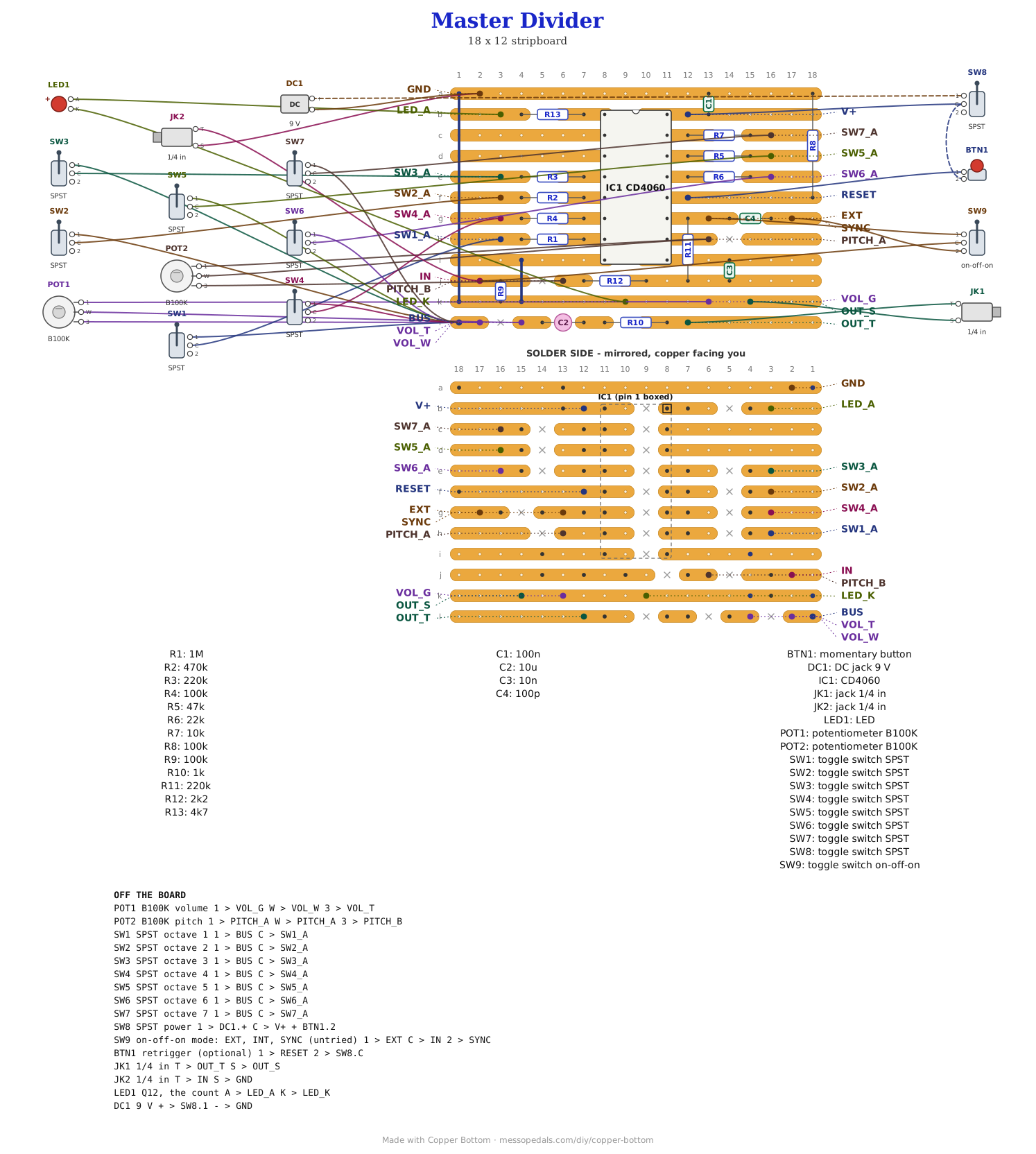
The Master Divider is a Grub that needs nothing plugged into it. A CD4060 is a chain of flip-flops with an oscillator built into the same chip, so it is its own clock: a pitch knob sets how fast, and seven octaves below it come out on seven switches through the Grub's weighted resistors onto one bus. An LED blinks with the count. On my breadboard it clicks rhythmically, exactly like the original divider, but with the oscillator underneath. This is the same circuit on a 12 × 18 board, with the same parts and the same reference numbers.
What you'll need
tap to expand / collapse
Nineteen parts on the board, counting two wire links. They are the breadboard guide's parts with the breadboard guide's reference numbers, so the two pages read the same.
- 1× CD4060 14-stage ripple counter with oscillator, 16-pin DIP (IC1) - spot it: sixteen legs, 4060 in the part number, a notch at one end. A CD4040 or CD4020 looks the same and has no oscillator; it will not run on its own. A socket is worth it
- The weighted ladder, one resistor per octave and every value different (R1 to R7): 1M (brown-black-green), 470K (yellow-violet-yellow), 220K (red-red-yellow), 100K (brown-black-yellow), 47K (yellow-violet-orange), 22K (red-red-orange), 10K (brown-black-orange). R1 is on Q4, the highest and quietest octave, and R7 on Q10, the lowest and loudest
- 2× 100K resistor (R8, R9) - spot it: brown-black-yellow, the same as the ladder's R4. R8 holds RESET low so the chip runs; R9 is the input pull-down
- 1× 220K resistor (R11) - spot it: red-red-yellow, the same as the ladder's R3. This one is Rs, from pin 11 to the timing node
- 1× 2.2K resistor (R12) - spot it: red-red-red. The floor under the pitch pot, not optional: at one end of the pot's travel it is the only timing resistor there is
- 1× 4.7K resistor (R13) - spot it: yellow-violet-red. Q12 to the LED
- 1× 1K resistor (R10) - spot it: brown-black-red. On the output, after the cap
- 1× 100nF ceramic (C1) - spot it: printed 104. Across the supply, beside the chip
- 1× 10nF ceramic (C3) - spot it: printed 103. The timing cap: this and the pitch knob set the speed of everything
- 1× 100pF ceramic (C4) - spot it: a tiny disc printed 101. The SYNC cap. It does nothing unless the mode switch picks SYNC
- 1× 10 µF electrolytic (C2) - spot it: a small can, stripe on the minus leg. Blocks the DC on the way out
- 2× wire links (J1, J2) - offcuts of component leg. J1 runs down the left edge and joins the top strip to the ground strip; J2 takes pin 8 down to ground
- 1× stripboard, 12 strips × 18 holes or larger
Off the board
- 1× B100K linear pot - PITCH, wired as a variable resistor: the wiper and one outer lug tied together to PITCH_A, the other outer lug to PITCH_B. R12 on the board is its stop
- 1× B100K linear pot - VOLUME, a divider, all three lugs
- 1× LED, any color - it blinks with the count. Its resistor is on the board
- 7× SPST switches, one per octave
- 1× on-off-on toggle - MODE, optional and untried. Middle is INT, the chip on its own clock; one side is EXT, the other SYNC. Leave it off and the board runs INT, which is how I built it
- 1× momentary switch between RESET and V+ - optional. Hold it and the chip stops; let go and the count starts again from the top
- 2× 1/4″ jack - IN and the output
- 1× DC jack, 9 V, or a battery snap. A CD4060 runs anywhere from 3 to 15 V
- An SPST toggle for power, in the positive supply lead between the DC jack and the board's V+ pad. Not in the layout file - it is off the board, and every build on this shelf gets one
The layout file is the guide
Like every layout on this shelf, the build document for this one is the file itself: ↓ Download Master_Divider.json - import it into Copper Bottom and the editor gives you the board picture, the placement walkthrough, the electrical checks and a printable build sheet, all from the same file. No coordinates are written out on this page on purpose: the editor is the viewer, and a number typed twice is a number that can drift.
How the strips go. Strip a is ground and strip k is ground, joined by J1 down the left edge. The chip stands across strips b to i, pin 1 at the top, and the right half of strip b is V+. The oscillator's three parts meet on strip j: R11 down from pin 11, C3 down from pin 9, and R12 out to the pitch pot. Strip l is the output. Q13 and Q14, pins 2 and 3, go nowhere and that is correct - an unused output needs nothing.
The netlist
Quoted verbatim from the layout file, and emitted from the copper rather than typed
beside it - so checking the board against it can only pass. What it is for is carrying the
circuit somewhere else, and telling you what each strip is doing while you stare at it. The
oscillator is RX, CX, CLK_IN and NODE.
The off-board wiring
Nineteen pads carry the build itself. Four more are optional: IN, EXT and SYNC for the input jack and the mode switch, and RESET for the retrigger.
| Pad | Goes to |
|---|---|
| V+ / GND | The supply, through the power toggle. DC jack positive to the toggle and the toggle's common to V+; negative to GND, which is also the input jack's sleeve |
| PITCH_A / PITCH_B | The PITCH pot, a variable resistor: the wiper and one outer lug tied together to PITCH_A, which is pin 10; the other outer lug to PITCH_B, which reaches the timing node through R12 |
| SW1_A … SW7_A / BUS | The seven octave switches. SW1 is Q4, the clock divided by 16, down to SW7, Q10, divided by 1024. Each switch's other side goes to the BUS pad, which is where they all sum |
| VOL_T / VOL_W / VOL_G | Volume pot, all three lugs |
| OUT_T / OUT_S | Output jack, tip and sleeve |
| LED_A / LED_K | The LED: long leg to LED_A, short leg to LED_K |
| IN | The input jack's tip, and the mode switch's middle lug. R9 holds it low, so an empty jack is quiet |
| EXT / SYNC | The mode switch's outer lugs, optional and untried. EXT goes straight to pin 11, so the input replaces the clock; SYNC reaches pin 11 through C4, so the input only tugs at it. Leave both empty and the board runs on its own clock |
| RESET | Pin 12, held low by R8. A momentary to V+ is the retrigger, or leave it empty |
How it works, in one breath
Inside a CD4060 is a pair of inverters waiting to be an oscillator and a chain of fourteen flip-flops waiting to be clocked. Pin 10 drives the pitch pot and R12 into the timing node, pin 9 drives C3 into the same node from the other side, and R11 feeds the node back into pin 11, so the chip clocks itself. Every flip-flop halves what it is given, and the chip brings out Q4 to Q10, seven octaves in a row, the first one already the clock divided by 16. Each goes through its own ladder resistor to its own switch and onto one bus, 1M down to 10K, so the high octaves sit on top of the low ones instead of burying them - the Grub's trick. Q12, two octaves below the bottom switch, is slow enough to see, so it drives the LED.
Things to try
None of these have been tried on this board, because this board has not been built.
- The mode switch. Fit the on-off-on and feed IN something high - the Mosquito 556, an Atari Punk Console, is the obvious one. EXT makes it the clock; SYNC only kicks the chip's own.
- Swap the timing cap. 1nF at C3 moves everything up ten times; 100nF moves it down ten times and the whole board becomes a rhythm.
- Gate it from outside. RESET held high stops the oscillator, so a slow square from another build on the RESET pad chops it into bursts. Share the grounds.
This one is mine: the Grub's weighted switch-and-bus mix on a CD4060, with the oscillator hookup from TI's CD4060B datasheet. The layout is mine, drawn in Copper Bottom, and so is anything wrong with it.