Dual-Wave LFO
One NE5532, a triangle and a square at once, and a knob that blends them · By Onion Madder · Mess O' Pedals
Two op-amps chasing each other. One integrates - it charges a capacitor at whatever rate you feed it, so its output ramps in a straight line. The other is a comparator with hysteresis: it watches that ramp and slams its own output to the opposite rail the moment the ramp crosses a threshold, which reverses the charging and sends the ramp back the other way. Neither one oscillates. Wired to each other they cannot do anything else. You get a triangle on pin 1 and a square on pin 7 at the same frequency, at the same time, and a 1K pot blends between them - all the way over is one shape, all the way back is the other, and the middle is whatever lopsided thing lives between. It is the same circuit as the breadboard Dual-Wave LFO, soldered down.
What you'll need
tap to expand / collapse
- 1× NE5532 dual op-amp, 8-pin DIP - spot it: 5532 in the part number, a notch at one end and a dot beside pin 1. An LM358 is the same pinout and is actually specified for a 9V supply - see the supply note below before you choose
- 1× 47K resistor (R1) - sets the fast end of the rate sweep. Spot it: bands yellow-violet-orange
- 1× 68K resistor (R2) - trigger window, triangle side. Do not swap with the 100K. Spot it: bands blue-gray-orange
- 2× 10K resistors (R3, R4) - the mid-rail divider; a matched pair matters more than the exact value. Spot them: bands brown-black-orange
- 1× 100K resistor (R5) - trigger window, feedback side. It is the one part on this board that stands on end, across two holes. Spot it: bands brown-black-yellow
- 1× 1 µF film capacitor (C1) - the integrator cap. It sets the rate, so film, not ceramic. Spot it: a little box or oblong, either way round
- 1× 47 µF electrolytic, 16V or higher (C2) - holds the half rail still. Spot it: a little can; the stripe marks the minus leg, which goes to ground
- 1× 100nF ceramic (C3) - supply decoupling, one hole from pin 8. Spot it: printed 104
- Stripboard, at least 16 holes by 8 strips, and four short lengths of wire for the links
Off the board
- 1× 100K linear pot (VR1) - rate. Spot it: marked B100K. Only the wiper and lug 3 are used; the third lug stays empty
- 1× 1K linear pot (VR2) - blend. Spot it: marked B1K or B102. All three lugs, and its wiper is the LFO output - that wire never touches the board
- 1× output lead or jack - tip to the VR2 wiper, sleeve to GND
- 1× DC jack or battery snap - 9–15V, and 12 to 15V is the better choice here at no cost in rate. See the supply note
The layout file is the guide
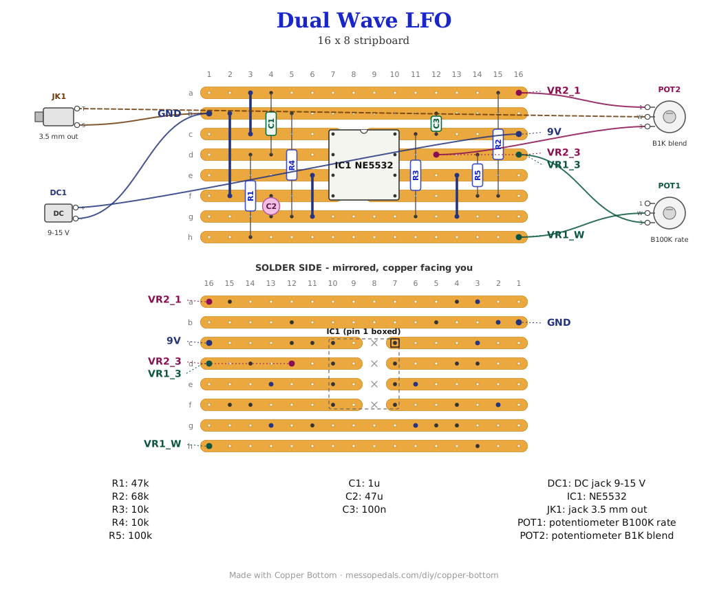
Like the 555 theremin and the Cicada NAND, the build document for this one is the file itself: ↓ Download Dual_Wave_LFO.json - import it into Copper Bottom and the editor gives you the board picture, the placement walkthrough, the electrical checks and a printable build sheet, all from the same file. No coordinates are written out on this page on purpose: the editor is the viewer, and a number typed twice is a number that can drift.
The chip, at a glance
The netlist
Quoted verbatim from the layout file. It was written from the board, so checking the board against it can only pass - what it is for is carrying the circuit somewhere else, and telling you what each strip is supposed to be doing while you stare at it.
The chip is doing most of the routing. The cut column splits each of the four strips the DIP straddles into two separate nodes, one pin on each side - so V+, ground, the triangle, the square, the integrator input and the comparator input are all just copper the chip is already sitting on. The one pair the circuit wants joined is pins 3 and 6, both of which want the half rail, and they are the one pair the cut separates. That is what J1 and J2 are for, and it is the only place this board needs a link at all.
The off-board wiring
Six pads leave the board: two pots, the supply and ground.
| Pad | Goes to |
|---|---|
| 9V / GND | The supply. 9 to 15V, positive to 9V and negative to GND. GND is also the output jack sleeve. The two pads sit on opposite edges of the board on purpose |
| VR1_3 / VR1_W | The rate pot, 100K linear. Lug 3 to VR1_3, the wiper to VR1_W, the third lug empty. It is a variable resistor in the charging path: the square wave drives lug 3, and how much of it reaches the integrator through R1 is the rate |
| VR2_1 / VR2_3 | The blend pot, 1K linear. Lug 1 to VR2_1 (the triangle) and lug 3 to VR2_3 (the square). Both outer lugs, both on the board |
| the VR2 wiper | This is the output, and there is no pad for it - the wiper goes straight to the jack tip and never touches copper. There is no OUT pad on this board because the pot is the output |
Do not swap R2 and R5. 68K on the triangle side and 100K on the feedback side set the trigger window. The other way round the window is wider than the swing, so the comparator never reaches its threshold and nothing starts at all - it just sits there with the triangle parked against a rail. It is the one mistake on this board that looks like a dead chip and is not.
The 9V problem
An NE5532 is specified from ±3V, which is 6V across the two supply pins, and it is below spec on a 9V battery once you account for the swing it is being asked to make. It will usually run. It will also be the first thing to blame when the triangle looks clipped or the rate goes strange as a battery sags. 12 to 15V is the better choice, and it costs nothing in rate: the trigger window is a ratio of R2 against R5, so it scales with the supply and the frequency stays where it was.
If 9V is what you have, an LM358 drops into the same eight holes - same pinout, actually specified for a single 9V rail, and slower and noisier in a way that does not matter at all for something making a wobble. Four salvaged vape cells in series land at 14.8V nominal, inside the good window, though nobody has run this board on them.
How it works, in one breath
R3 and R4 make a half rail and C2 holds it still, and both non-inverting-ish inputs that need a reference sit on it - pin 3 for the integrator and pin 6 for the comparator. Op-amp B is the comparator: its output at pin 7 is already hard against one rail, R5 feeds some of that back to pin 5, and R2 brings the triangle in alongside it, so pin 5 sits at a mix of the two. When the triangle has moved far enough to drag that mix past the half rail, pin 7 flips, which flips what R5 is contributing, which moves the threshold to the other side - that is the hysteresis, and it is why it snaps rather than dithers. Op-amp A is the integrator: the square arrives through VR1 and R1 into pin 2, C1 sits between pin 2 and pin 1, and a constant current into a capacitor is a straight ramp. Each half produces exactly what the other one needs to keep going.
Things to try
- A bigger C1 for a slower sweep, or a smaller one to push it up toward audio. It is a straight trade against the rate pot and nothing else in the circuit cares
- The square is a rail-to-rail logic-level signal, so it will clock a Grub Divider or a Spider Sequencer straight off VR2_3 - take it before the blend pot, not after
- The triangle into a vactrol is the tremolo this board does not have. The Optical Tremolo builds its own LFO for exactly that job; this one would replace it and give you both shapes
- A second blend pot fed from the same two pads, so one box has two outputs at different mixes of the same wave. Untested, and it loads both outputs - the 1K is low enough that two in parallel is 500R across them
↓ Same box, jacks on top (PDF)
The second sheet keeps both pots where this one has them and moves the jacks - power and audio - to the top wall, so the cables leave upward. Two ways to drill one box; pick one.
Print at 100% / “Actual size”, never “Fit to page” - check the bar measures exactly 4″ before you touch a drill. The face is 66 by 121 mm but only 42 mm of it is drillable once the lid lip is clear.
Nobody has drilled this one yet. The hole sizes come from the parts; where they sit is this format applied to them. Offer the sheet up to the box and check it against your own parts before you make a hole.
The triangle-and-square pair is an old one and belongs to nobody - this version of it came from the Experimentalists Anonymous archive. The breadboard build, this layout and the box are Onion Madder's, drawn in Copper Bottom.