Cricket
Two CD4001 NOR chips: two tones, one slow chop, a play and stop latch · By Onion Madder · Mess O' Pedals
A CD4001 is four two-input NOR gates, and a NOR gate has one rule: its output is high only when both inputs are low. Everything this box does falls out of that. It has no Schmitt trigger, so an oscillator takes two gates, not one, and each oscillator keeps a spare input that stops it dead when you pull it high. Two chips is eight gates: a slow oscillator, two tones, and a two-gate latch. The slow one chops either tone or both, through a toggle each; the latch is a PLAY button and a STOP button, no power switch needed to make it shut up. The two tones sum onto one volume knob. Named for the cricket, whose whole song is a tone chopped by a slow pulse, which is what this is.
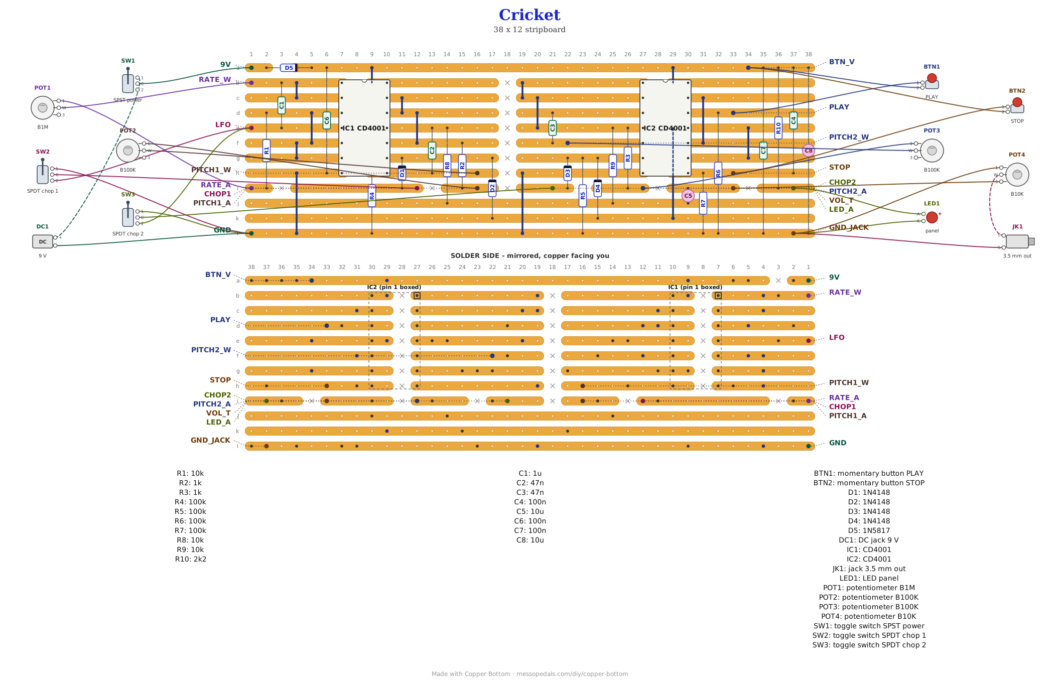
What you'll need
tap to expand / collapse
- 2× CD4001 quad two-input NOR, 14-pin DIP - spot it: 4001 somewhere in the part number (CD4001BE, HEF4001, MC14001), notch marks pin 1. Same pinout as the 4011 and the 4093, so do not grab one of those by feel
- 1× 1N5817 Schottky - spot it: black body, silver band. Reverse-polarity protection on the supply
- 4× 1N4148 - spot it: small glass body, black band. Two per tone, the diode-OR that lets either the latch or the chop silence it
- 5× 100K (brown-black-yellow) - the four pull-downs and nothing else. R4 and R5 hold the two stop inputs low, R6 and R7 hold the two buttons low
- 3× 10K (brown-black-orange) - the LFO's floor under the rate pot, and the two mix resistors
- 2× 1K (brown-black-red) - the floors under the two pitch pots, so a knob at zero cannot short a gate's output to its own input
- 1× 2K2 (red-red-red) for the LED
- 1× 1 µF film (105) - the LFO's timing cap. Film, not electrolytic: the LFO swings it both ways
- 2× 47nF ceramic (473) - the two tone timing caps
- 3× 100nF ceramic (104) - one decoupling cap per chip, and one from STOP to V+ that resets the latch at power-on
- 2× 10 µF electrolytic - the output coupler and the supply bulk. Spot it: the stripe marks the negative leg
- 1× stripboard, 12 strips × 38 holes or larger, and wire for fourteen links, six of them one hole long
Off the board
- 1× 1M linear pot (B1M) - RATE. Two lugs
- 2× 100K linear pot (B100K) - PITCH 1 and PITCH 2. Two lugs each
- 1× 10K linear pot (B10K) - VOLUME. All three lugs; the wiper is the output jack
- 2× SPDT toggles - CHOP 1 and CHOP 2, drone or chop
- 2× momentary pushbuttons, normally open - PLAY and STOP
- 1× LED for the panel, any color - power
- 1× 3.5 mm jack - out
- 1× DC jack or a 9V battery snap, and an SPST toggle for power
- An upright 125B - the drill template further down
The layout file is the guide
Like the 555 theremin and the Cicada NAND, the build document for this one is the file itself: ↓ Download Cricket.json - import it into Copper Bottom and the editor gives you the board picture, the placement walkthrough, the electrical checks and a printable build sheet, all from the same file. No coordinates are written out on this page on purpose: the editor is the viewer, and a number typed twice is a number that can drift.
The netlist
Quoted verbatim from the layout file. It was written from the board, so checking the board against it can only pass - what it is for is carrying the circuit somewhere else, and telling you what each strip is supposed to be doing while you stare at it.
The off-board wiring
Seventeen pads leave the board. Four pots, three toggles, two buttons, an LED, a jack and the supply.
| Pad | Goes to |
|---|---|
| 9V / GND | The supply, 9V, through the power toggle: DC jack positive to one side of the toggle, the other side to 9V. GND is the supply negative, and also the drone position of both chop toggles |
| RATE_A / RATE_W | The rate pot, 1M. One outer lug to RATE_A, the wiper to RATE_W, the third lug empty. A variable resistor with its 10K floor on the board, so the LFO cannot be turned into a dead short |
| PITCH1_A / PITCH1_W | The first pitch pot, 100K, wired the same way. Its 1K floor is on the board |
| PITCH2_A / PITCH2_W | The second pitch pot, the same again |
| CHOP1 / CHOP2 | The common lug of each chop toggle. One throw to GND, the other to LFO. Toward GND the tone drones; toward LFO the slow oscillator chops it |
| LFO | The slow oscillator's square, straight off the chip. Both chop toggles take their LFO throw from here. It will also drive a jack through a 1K if you want a clock out for the Spider or the Grub |
| PLAY / STOP / BTN_V | The two buttons. One side of PLAY to the PLAY pad, one side of STOP to the STOP pad, and the other side of both to BTN_V, which is V+. Pressing one pulls its input high; the pull-downs on the board hold them low the rest of the time |
| VOL_T / GND_JACK | The volume pot, 10K. Lug 3 to VOL_T, lug 1 to GND_JACK, and the wiper goes straight to the output jack tip. The jack sleeve and the LED cathode go to GND_JACK too. There is no OUT pad: the pot is the output |
| LED_A | The power LED's anode, through the 2K2 on the board. Cathode to GND_JACK |
The board comes up silent. The 100nF from STOP to V+ pulls the STOP input high for a moment when power arrives, so the latch always wakes up in the stopped state. Press PLAY and both tones start; press STOP and they both stop, in whatever chop setting they were in. That is the whole point of spending two gates on a latch: the box has a power switch for the battery and a separate start and stop for the sound.
How it works, in one breath
A NOR with its two inputs tied together is an inverter. Take two of them: the first one's output into the second, a cap from the second one's output back to the first one's input, and a resistor from the first one's output to its own input. The cap charges through the resistor until the first gate flips, both outputs swap, and it charges back the other way. That is a square wave at about 1 / (2.2 R C), and there are three of them on this board. The rate pot with its 10K floor and the 1 µF give the LFO roughly 0.4 to 40 times a second; the pitch pots with their 1K floors and 47nF give the tones roughly 100 Hz to 10 kHz. Ballpark numbers, because a CMOS threshold is not exactly half the rail.
The trick is the spare input. Each tone's first gate uses one input as its timing node and the other as a control: hold that control low and the gate is an inverter and the tone runs; pull it high and the gate's output is forced low no matter what, and the tone stops. Two diodes bring two different highs to that input and a 100K holds it low when neither is there. One diode comes from the chop toggle, which hands it either ground or the LFO's square, so the tone runs on the LFO's low half and stops on its high half. The other comes from the latch.
The latch is the last two gates cross-coupled: each one's output feeds the other's spare input. A high on PLAY forces one output low, which lets the other go high, and the pair holds that way after you let go. STOP does the same the other way round. The output that goes high when stopped is Qbar, and it runs along a bus strip to both tones' diodes, so stopped means both tones silenced regardless of the toggles. The two tones each drop through a 10K onto the MIX strip, the sum leaves through a 10 µF into the volume pot, and the 2K2 and LED just say the power is on.
Unbuilt, and these are the bench numbers. The frequency ranges, which will land wherever the gates' thresholds put them. Whether the LFO's chop has an audible click at the edges when the toggle is thrown toward it, and whether that is a feature. Whether the power-on reset always wins, or whether a slow supply ramp lets the latch come up playing now and then; if it does, the 100nF grows. And how loud two full-rail squares through 10K each are into whatever comes next: hot, is the guess. The floor resistors are the ones not to leave out, for the same reason as on the Hive and the Cicada - a pot at zero would tie a gate's output to its own input.
Things to try
- The chop is the LFO's low half. Swap one tone's CHOP wire from LFO to the LFO's other gate output and the two tones alternate instead of chopping together. Untested; it wants a pad the board does not have, so it is a wire to a chip pin
- A bigger LFO cap, 4.7 µF, for a chop slow enough to be a rhythm rather than a tremolo. Film or a bipolar electrolytic; the node swings both ways
- A third toggle that hands one chop input the other tone instead of the LFO, so tone 2 chops tone 1 at audio rate. That is the harsh gated sound the Cicada gets from a NAND, with the opposite polarity
- The Eurorack version, once this one is heard: the LFO and the latch are the rack-native parts of it, a clock and a gate
↓ Same box, jacks on top (PDF)
The second sheet keeps every control where this one has it and moves the jacks - power and audio - to the top wall, so the cables leave upward. Two ways to drill one box; pick one.
Print at 100% / “Actual size”, never “Fit to page” - check the bar measures exactly 4″ before you touch a drill. The face is 66 by 121 mm but only 42 mm of it is drillable once the lid lip is clear.
Nobody has drilled this one yet. The hole sizes come from the parts; where they sit is this format applied to them. Offer the sheet up to the box and check it against your own parts before you make a hole. The button holes are drawn for 12 mm panel momentaries; measure yours.
The two-gate CMOS oscillator is as old as CMOS and belongs to nobody. What is done with eight of the gates here - the chop, the diode-OR stop inputs, the latch with its power-on reset - and the layout and the box are Onion Madder's, drawn in Copper Bottom.