Rungler
Two oscillators, eight bits, and a pattern that eats itself · By Onion Madder · Mess O' Pedals
A Rungler is Rob Hordijk's idea, the heart of his Benjolin: take two oscillators, let one clock a shift register and the other feed it bits, turn the last few bits of the register back into a voltage, and use that voltage to bend the pitch of the very oscillators making the bits. The loop closes on itself and what comes out is a pattern that is never quite random and never quite repeats. This is a small one on the chips a noise box already has: a 40106 for the two oscillators, a CD4094 for the eight bits, a CD4070 for the XOR that stirs new bits in and for a second XOR that ring-modulates the two oscillators into the mix. Two pitch knobs, two depth knobs for how hard the pattern bends each pitch, a level knob, and a toggle that either lets the pattern keep mutating or locks it into an eight-step loop.
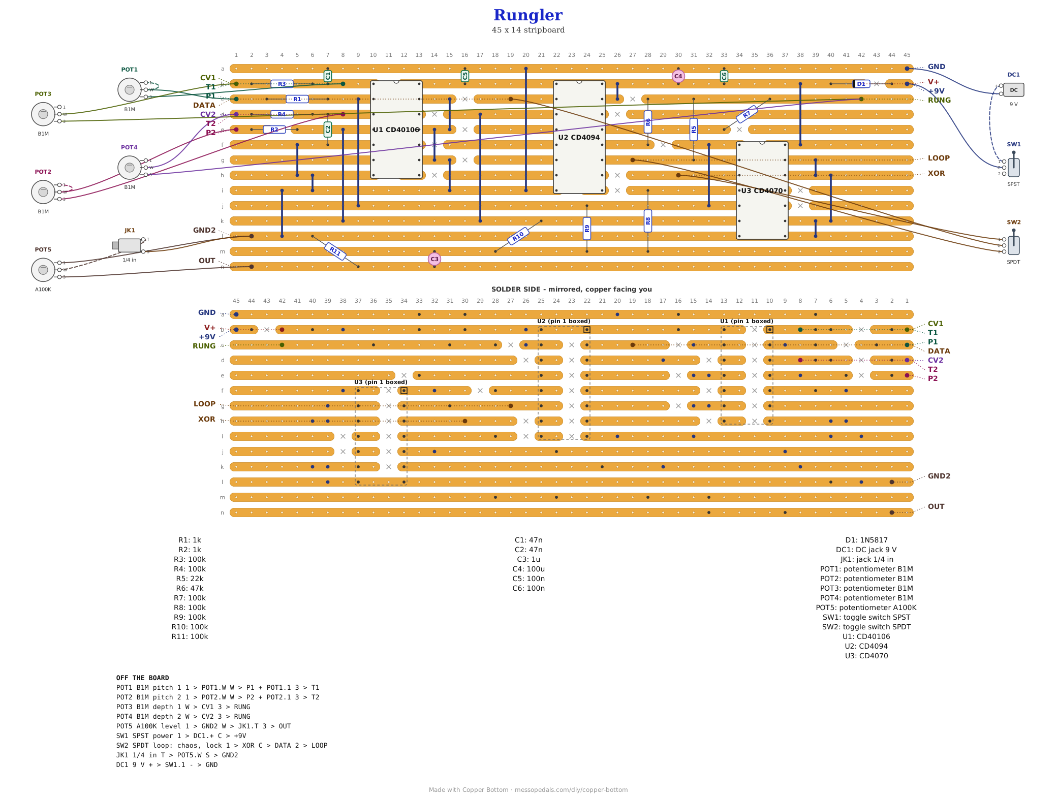
What you'll need
tap to expand / collapse
Eighteen parts on the board plus the links, and nine off it. Three chips, all ordinary 4000-series.
- 1× CD40106 hex Schmitt inverter, DIP-14 (U1) - spot it: fourteen legs, the number printed on top, a notch at one end. Two gates are the two oscillators; the other four are tied off. Fit a socket
- 1× CD4094 8-stage shift-and-store register, DIP-16 (U2) - spot it: sixteen legs, notch at one end. Eight bits that walk along on every clock. Its strobe and output-enable pins are tied high on the board so it is always transparent. Fit a socket
- 1× CD4070 quad XOR, DIP-14 (U3) - spot it: fourteen legs, notch at one end. Two gates used, two tied off. A CD4030 is the same thing under an older number. Fit a socket
- 1× 1N5817 Schottky (D1) - spot it: fat black body, a gray band at one end. Reverse-polarity protection on the supply
- 7× 100K resistor (R3, R4, R7, R8, R9, R10, R11) - spot it: bands brown-black-yellow. Six jobs. R3 and R4 carry each depth pot into its oscillator's timing node; R7 is the smallest bit of the three-bit ladder; R8, R9 and R10 are the mixer, one per voice; R11 ties the output down
- 1× 47K resistor (R6) - spot it: bands yellow-violet-orange. The middle bit of the ladder, from Q7
- 1× 22K resistor (R5) - spot it: bands red-red-orange. The biggest bit of the ladder, from Q8. 22K, 47K, 100K is the whole DAC: three bits, binary weighted, summed on the RUNG pad
- 2× 1K resistor (R1, R2) - spot it: bands brown-black-red. One in series with each pitch pot, so an oscillator can never see zero ohms
- 2× 47nF ceramic (C1, C2) - spot it: printed 473. The two timing caps, one per oscillator. Same value, so the two knobs cover the same range
- 2× 100nF ceramic (C5, C6) - spot it: printed 104. One decoupling cap per chip pair
- 1× 1 µF electrolytic (C3) - spot it: a small can with a stripe down one side; the stripe leg is the negative one. The output coupling cap. Stripe toward the level pot
- 1× 100 µF electrolytic (C4) - spot it: a small can with a stripe down one side; the stripe leg is the negative one. The supply reservoir. Stripe to ground
- 16× wire links - offcuts of component leg
- 1× DIP-16 socket and 2× DIP-14 sockets
Off the board
- 2× B1M linear pots - pitch 1 and pitch 2. Variable resistors: lug 3 to T1 or T2, wiper to P1 or P2, wiper jumpered to lug 1. The 1K each needs is on the board
- 2× B1M linear pots - depth 1 and depth 2, how hard the pattern bends each pitch. Variable resistors from the ladder: lug 3 of both to RUNG, wipers to CV1 and CV2, lug 1 empty
- 1× A100K log pot - level. Lug 3 to OUT, lug 1 to GND2, wiper to the output jack tip
- 1× SPDT toggle - loop. Center to DATA; one side to XOR, where the pattern keeps mutating, the other to LOOP, where it locks and repeats
- 1× 1/4 inch jack - out. Tip to the level wiper, sleeve to GND2
- 1× DC jack, 9 V center negative
- An SPST toggle for power, in the positive supply lead between the DC jack and the board's +9V pad. Every build on this shelf gets one, and the drawing above shows it
The layout file is the guide
Like every layout on this shelf, the build document for this one is the file itself: ↓ Download Rungler.json - import it into Copper Bottom and the editor gives you the board picture, the placement walkthrough, the electrical checks and a printable build sheet, all from the same file. No coordinates are written out on this page on purpose: the editor is the viewer, and a number typed twice is a number that can drift.
Two ground strips, one net. Strip a carries the GND pad at the top right and strip l the GND2 pad at the bottom left, and the rest of the ground net reaches them through links. The V+ pad at the top right is a test point - nothing leaves the board there. It sits on the protected side of D1, on the net where the 4094's STROBE, OE and VDD pins meet, and its job is to tell the checker that net is a supply; without it those three pins read as a short.
The netlist
My script wrote this from the design and the board was checked against it in Copper Bottom: every connection it names is on the board and nothing on the board is missing from it. The three lines that are the Rungler are Q8, the register's last bit going to the loop toggle, to the XOR and into the ladder; RUNG, where the three ladder resistors meet and the depth pots take it; and O2, the second oscillator clocking the register. MIX is three 100K resistors: oscillator 1, oscillator 2, and their XOR.
The off-board wiring
Fifteen pads leave the board, one of them a test point: five pots, a toggle, the jack and the supply.
| Pad | Goes to |
|---|---|
| T1 / P1, T2 / P2 | The two B1M pitch pots. Lug 3 to T, wiper to P, wiper jumpered to lug 1. Variable resistors; R1 and R2 are their 1K floors |
| RUNG / CV1 / CV2 | The two B1M depth pots. Lug 3 of both to RUNG, the stepped voltage; wipers to CV1 and CV2, which go through 100K into each oscillator's timing node. Lug 1 empty. Fully off, the pattern does not touch that pitch |
| DATA / XOR / LOOP | The loop toggle. Center to DATA, the register's input. XOR feeds it oscillator 1 XORed with the last bit, so new bits keep arriving; LOOP feeds it the last bit straight back, so the eight bits circulate unchanged |
| OUT | Level pot lug 3. The wiper goes to the output jack tip, and lug 1 to GND2 |
| GND2 | Level pot lug 1 and the jack sleeve. Same net as GND |
| V+ | A test point on the protected supply after D1. Nothing lands here |
| +9V / GND | The supply, through the power toggle. DC jack positive to the toggle and the toggle to +9V; negative to GND |
How it works, in one breath
Two gates of the 40106 are two oscillators, each a 1M pot plus 1K back from its output to its input with 47n to ground, so each runs from under twenty hertz to well up in the kilohertz. Oscillator 2 clocks the 4094: on every rising edge the eight bits shift one place and a new bit is read at DATA. Where that bit comes from is the toggle. In LOOP it is Q8, the bit falling off the end, so the same eight bits go round forever and you get an eight-step pattern. In XOR it is oscillator 1 XORed with Q8: oscillator 1 is running at its own unrelated rate, so whether it is high or low at each clock is as good as a coin, and the XOR against the old bit means the pattern is always being rewritten out of itself. The last three bits, Q6, Q7 and Q8, go through 100K, 47K and 22K to one node, RUNG: a three-bit ladder, eight steps of voltage, changing on every clock.
That voltage is what bends the pitches. Each depth pot takes RUNG and feeds it through 100K into an oscillator's timing node, so every step of the ladder pushes that oscillator sharp or flat by however much the depth knob allows. Bend oscillator 2 and the clock itself speeds and slows with the pattern it is producing; bend oscillator 1 and the coin gets weighted. That is the loop Hordijk built, and it is why a Rungler never settles. The output is a mix of the two oscillators and their XOR, which is the two ring-modulated, through the level pot. That is what the schematic does, and it is a read of the circuit, not of a build; what it sounds like in the middle of the depth knobs is the thing nobody has heard yet.
Things to try
None of these have been tried, because none of this has. They are the obvious knobs.
- A voltage out. RUNG is a stepped control voltage already; a 3.5 mm jack on it, through 10K, drives the Envelope Filter or anything else with a CV in
- Different timing caps. 47n on one oscillator and 470n on the other puts the clock in LFO territory and the data oscillator at audio, which is closer to the Benjolin's proportions
- Change the ladder. 10K, 22K, 47K makes the steps bigger; 100K, 220K, 470K makes them subtler
- Take Q1 to Q5 out to five more resistors and toggles and it is a gate sequencer as well
The Rungler is Rob Hordijk's, from the Benjolin, and the name is his too. His used a 4021 and its own oscillators and a different ladder; this small one on a 4094 and a 40106, and the layout, are mine, and so is anything wrong with them.