XOR Cross-Mod
Three pitch knobs, one toggle, digital ring modulation · By Onion Madder · Mess O' Pedals
An XOR gate is a ring modulator for square waves: its output is high when its two inputs differ, so feed it two oscillators and out comes the sum and the difference of their pitches and none of the originals, metallic and bell-like when the two are close, a clang when they are not. This board is three 40106 oscillators on three pitch knobs and two gates of a CD4070. The first gate XORs oscillators 1 and 2. The second XORs that result with oscillator 3. A toggle picks which of the two you hear, so it is two voices cross-modulated, or all three, and with three knobs the beating between them is the instrument. Smallest board of the six.
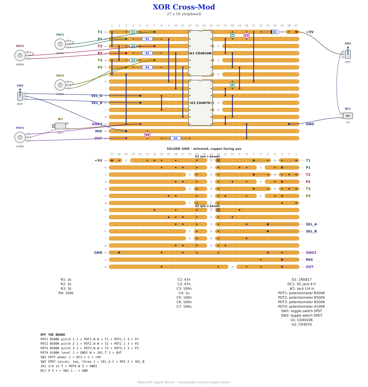
What you'll need
tap to expand / collapse
Twelve parts on the board plus the links, and eight off it.
- 1× CD40106 hex Schmitt inverter, DIP-14 (U1) - spot it: fourteen legs, the number printed on top, a notch at one end. Three gates are the three oscillators; the other three are tied off. Fit a socket
- 1× CD4070 quad XOR, DIP-14 (U2) - spot it: fourteen legs, notch at one end. Two gates used, two tied off. A CD4030 is the same thing under an older number. Fit a socket
- 1× 1N5817 Schottky (D1) - spot it: fat black body, a gray band at one end. Reverse-polarity protection on the supply
- 1× 100K resistor (R4) - spot it: bands brown-black-yellow. Ties the output to ground so the level pot has something to sit on
- 3× 1K resistor (R1, R2, R3) - spot it: bands brown-black-red. One in series with each pitch pot, so an oscillator can never see zero ohms
- 2× 47nF ceramic (C1, C2) - spot it: printed 473. The timing caps for oscillators 1 and 2. Equal, so the two knobs cover the same range
- 3× 100nF ceramic (C3, C5, C6) - spot it: printed 104. C3 is oscillator 3's timing cap, twice the other two, so its knob sits an octave lower; C5 and C6 decouple the chips
- 1× 1 µF electrolytic (C4) - spot it: a small can with a stripe down one side; the stripe leg is the negative one. The output coupling cap. Stripe toward the level pot
- 1× 100 µF electrolytic (C7) - spot it: a small can with a stripe down one side; the stripe leg is the negative one. The supply reservoir. Stripe to ground
- 16× wire links - offcuts of component leg
- 2× DIP-14 sockets
Off the board
- 3× B500K linear pots - pitch 1, 2 and 3. Variable resistors: lug 3 to P1, P2 or P3, wiper to T1, T2 or T3, wiper jumpered to lug 1. The 1K each needs is on the board
- 1× A100K log pot - level. Lug 3 to OUT, lug 1 to GND2, wiper to the output jack tip
- 1× SPDT toggle - voices. Center to MIX; one side to SEL_A for oscillators 1 and 2, the other to SEL_B for all three
- 1× 1/4 inch jack - out. Tip to the level wiper, sleeve to GND2
- 1× DC jack, 9 V center negative
- An SPST toggle for power, in the positive supply lead between the DC jack and the board's +9V pad. Every build on this shelf gets one, and the drawing above shows it
The layout file is the guide
Like every layout on this shelf, the build document for this one is the file itself: ↓ Download XOR_Cross_Mod.json - import it into Copper Bottom and the editor gives you the board picture, the placement walkthrough, the electrical checks and a printable build sheet, all from the same file. No coordinates are written out on this page on purpose: the editor is the viewer, and a number typed twice is a number that can drift.
The two chips stand one above the other, the 40106 on the upper strips and the 4070 on the lower, so the board is nearly square. Strip n carries ground, with the GND and GND2 pads at either end, and the 4070's ground pin sits straight on it. Every pad but the supply is down the left edge, so the pots and the toggle all wire to one side.
The netlist
My script wrote this from the design and the board was checked against it in Copper Bottom: every connection it names is on the board and nothing on the board is missing from it. Three lines are the whole circuit: O1, O2 and O3, each an oscillator's output going to its 1K, its XOR input, and nowhere else. X12 is the first XOR's output, on the toggle and into the second gate; X123 is the second's, on the toggle alone.
The off-board wiring
Thirteen pads leave the board: three pitch pots, the level pot, the toggle, the jack and the supply.
| Pad | Goes to |
|---|---|
| P1 / T1, P2 / T2, P3 / T3 | The three B500K pitch pots. Lug 3 to P, wiper to T, wiper jumpered to lug 1. Variable resistors; R1, R2 and R3 are their 1K floors |
| MIX / SEL_A / SEL_B | The voices toggle. Center to MIX, which is the output coupling cap. SEL_A is oscillators 1 and 2 through one XOR; SEL_B is that result through a second XOR with oscillator 3 |
| OUT | Level pot lug 3. The wiper goes to the output jack tip, and lug 1 to GND2 |
| GND2 | Level pot lug 1 and the jack sleeve. Same net as GND |
| +9V / GND | The supply, through the power toggle. DC jack positive to the toggle and the toggle to +9V; negative to GND |
How it works, in one breath
Three gates of the 40106 are three oscillators, each a 500K pot plus 1K back from its output to its input with a cap to ground: 47n on the first two, 100n on the third, so the third knob sits about an octave below the others over the same travel. Oscillator 1 goes to one input of the first XOR gate and oscillator 2 to the other. An XOR is high only when its inputs differ, so when the two square waves are at the same pitch and in step the output is silence, and as they drift apart the output flickers between them at the rate they beat: that flicker is the difference frequency, and the sum is in there too. It is exactly what a ring modulator does to two sine waves, done to squares with one gate.
The first gate's output goes to the toggle and also into the second gate, where oscillator 3 is the other input, so the second gate's output is all three cross-modulated. The toggle picks one or the other, C4 blocks the DC, and the level pot sets how much leaves. There is no mixing of the raw oscillators anywhere on the board: you never hear the three pitches, only what they do to each other, which is why the knobs feel nothing like tuning. That is what the schematic does, and it is a read of the circuit, not of a build.
Things to try
None of these have been tried, because none of this has. They are the obvious knobs.
- Mix the raw oscillators in. A 100K from O1, O2 or O3 to MIX puts a fundamental under the clang
- Change C3 to 470n and oscillator 3 becomes an LFO, and the toggle's second position is a tremolo on the first two
- Use the other two XOR gates. Pins 8 and 9 in, 10 out, and 12 and 13 in, 11 out, are sitting on ground waiting
- Send it to the CMOS Ladder Filter, which likes exactly this kind of signal
An XOR as a ring modulator for square waves is the standard Lunetta trick and belongs to everyone who has ever built one. Chaining two of them behind a toggle, and the layout, are mine and so is anything wrong with them.