CMOS Ladder Filter
One chip, one transistor, a cutoff knob that starves it · By Onion Madder · Mess O' Pedals
A lowpass filter with no resistors in the signal path. A CD4069 is six inverters, and an inverter with its output tied to its input sits at half the supply and behaves like a resistor to the middle, a few hundred ohms to a few thousand depending on how much voltage the chip is given. So each stage here is an inverter driving a node, a second inverter tied to itself to be the resistor, and a 47nF cap to ground. Three of those in a row is an 18 dB per octave ladder. The cutoff knob is the chip's supply: a transistor follows the pot and feeds the 4069 anywhere from about two and a half volts to about seven, the inverters get slower and softer as it drops, and the corner moves with it. Starving a chip on purpose, with a knob.
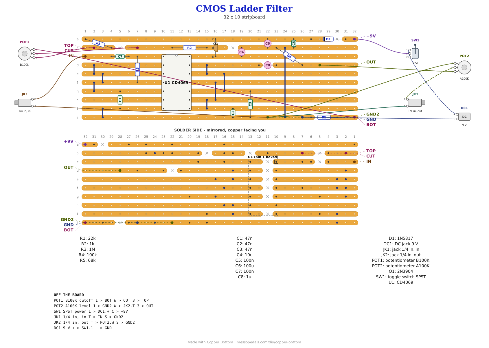
What you'll need
tap to expand / collapse
Fifteen parts on the board plus the links, and six off it. Nothing exotic, but the chip has to be the unbuffered one.
- 1× CD4069UBE hex inverter, DIP-14 (U1) - spot it: fourteen legs, the number printed on top, a notch at one end. It must be the unbuffered part, which every chip sold as CD4069UB or UBE is. A buffered inverter, a 74HC04 for one, snaps between the rails and cannot be held in the middle, and this whole circuit lives in the middle. Fit a socket
- 1× 2N3904 NPN transistor (Q1) - spot it: a black half-round TO-92 with the number on the flat face. The emitter follower that turns the cutoff pot's voltage into the chip's supply. Any small NPN will do; the legs are E-B-C with the flat face toward you
- 1× 1N5817 Schottky (D1) - spot it: fat black body, a gray band at one end. Reverse-polarity protection on the supply; a backwards plug does nothing
- 1× 1M resistor (R3) - spot it: bands brown-black-green. From the first inverter's output back to its input, which holds it in the linear region as the input amplifier
- 1× 100K resistor (R4) - spot it: bands brown-black-yellow. Ties the output to ground so the level pot has something to sit on
- 1× 68K resistor (R5) - spot it: bands blue-gray-orange. The bottom of the cutoff divider, so the pot can never pull the chip's supply all the way to nothing
- 1× 22K resistor (R1) - spot it: bands red-red-orange. The top of the cutoff divider, so it can never reach the full nine volts either
- 1× 1K resistor (R2) - spot it: bands brown-black-red. Into the transistor's base, from the cutoff wiper
- 3× 47nF ceramic (C1, C2, C3) - spot it: printed 473. The three filter caps, one per stage, to ground. Change all three together to move the whole range
- 2× 100nF ceramic (C5, C7) - spot it: printed 104. C7 is the input coupling cap; C5 decouples the raw supply
- 1× 1 µF electrolytic (C8) - spot it: a small can with a stripe down one side; the stripe leg is the negative one. The output coupling cap. Stripe to the output side
- 1× 10 µF electrolytic (C4) - spot it: a small can with a stripe down one side; the stripe leg is the negative one. Holds the chip's starved supply steady. Stripe to ground
- 1× 100 µF electrolytic (C6) - spot it: a small can with a stripe down one side; the stripe leg is the negative one. The supply reservoir. Stripe to ground
- 9× wire links - offcuts of component leg
- 1× DIP-14 socket
Off the board
- 1× B100K linear pot - cutoff. All three lugs: lug 3 to TOP, lug 1 to BOT, wiper to CUT. A divider, not a variable resistor: the ends are what keep the chip inside its supply range
- 1× A100K log pot - level. Lug 3 to OUT, lug 1 to GND2, wiper to the output jack tip
- 2× 1/4 inch jacks - in and out. Tips to IN and the level wiper, sleeves to GND2
- 1× DC jack, 9 V center negative. D1 means a backwards plug does nothing
- An SPST toggle for power, in the positive supply lead between the DC jack and the board's +9V pad. Every build on this shelf gets one, and the drawing above shows it
The layout file is the guide
Like every layout on this shelf, the build document for this one is the file itself: ↓ Download CMOS_Ladder_Filter.json - import it into Copper Bottom and the editor gives you the board picture, the placement walkthrough, the electrical checks and a printable build sheet, all from the same file. No coordinates are written out on this page on purpose: the editor is the viewer, and a number typed twice is a number that can drift.
Ground is the bottom strip. GND, GND2 and the cutoff pot's BOT pad all sit on strip j, and the three filter caps and the divider's bottom resistor return to it. At the very bottom of the cutoff knob the chip's supply dips under the three volts the datasheet gives as a 4069's floor, so expect the last of the travel to choke it, which may be the point. Copper Bottom will report three pin-short errors on U1. Read them before you dismiss them: each names one stage's node, where a driving output, a self-tied inverter and the next inverter's input all share a strip on purpose. If it reports a fourth, that one is real.
The netlist
My script wrote this from the design, not from the copper, and the board was checked against it in Copper Bottom: every connection it names is on the board and nothing on the board is missing from it. The lines to find are Y1, Y2 and Y3 - one per stage, each carrying two outputs and two inputs of the same chip, which is the whole trick - and VDDF, the chip's own supply pin hanging off the transistor's emitter.
The off-board wiring
Eight pads leave the board: the cutoff pot takes three, the level pot two, the two jacks and the supply the rest.
| Pad | Goes to |
|---|---|
| TOP / CUT / BOT | The B100K cutoff pot, all three lugs: lug 3 to TOP, wiper to CUT, lug 1 to BOT. It is a divider between R1 and R5, and the wiper sets the chip's supply through Q1 |
| IN | Input jack tip, through your bypass switch if you fit one. The sleeve goes to GND2 |
| OUT | Level pot lug 3. The wiper goes to the output jack tip, and lug 1 to GND2 |
| GND2 | Level pot lug 1 and both jack sleeves. Same net as GND, a second pad because the jacks are on that side |
| +9V / GND | The supply, through the power toggle. DC jack positive to the toggle and the toggle to +9V; negative to GND |
How it works, in one breath
The signal comes in through C7 to the first inverter, which R3 holds in the middle of its swing so it works as an amplifier. There is no input resistor, so its gain is set by whatever is plugged in, and with a guitar that is a lot: expect this stage to bite. Its output drives node Y1. On Y1 sits the second inverter with its output tied to its own input, which parks it at half the supply and makes it fight anything that tries to move the node, gently, like a resistor to the middle. With C1 to ground that is one lowpass pole. The third inverter reads Y1 and drives Y2, where the fourth inverter is the resistor and C2 the cap, and the fifth drives Y3 with the sixth as the resistor and C3 the cap. Three poles, three inversions, out through C8 to the level pot.
How strong that resistor is depends on the chip's supply voltage, because an inverter's transconductance does. That is the cutoff control: the pot is a divider between R1 and R5, its wiper goes through R2 into Q1's base, and Q1's emitter is the 4069's pin 14 with C4 to keep it steady. Turn the pot down and the chip runs on three volts, the inverters go weak and slow, the poles drop and the whole thing gets darker and quieter. Turn it up and it opens. The rest of the board runs on the full nine volts; only U1 is starved. That is a read of the circuit, not of a build, and the exact range and how it sounds at the bottom are the two things only a board can answer.
Things to try
None of these have been tried, because none of this has. They are the obvious knobs.
- Change the three 47n caps together. 100n moves the whole range down, 22n up. Change one and the poles spread instead
- Put a resistor in series with the input. 10K to 100K between C7 and pin 1 turns the first stage into a proper inverting amplifier with a gain you chose, if the bite is too much
- Swap R1 and R5 for other values to move the ends of the cutoff range. The chip will not do anything useful below about three volts, so keep R5 in
- Feed it a square wave. Any 40106 voice on this shelf into IN, and the filter does what a filter does to a square wave. The XOR Cross-Mod is the obvious partner
Using a 4069's inverters as resistors and starving the chip to move the cutoff is an old trick - the EDP Wasp built its filter that way in the seventies - and it belongs to whoever first noticed that an inverter tied to itself sits in the middle. The arrangement here, three stages on one chip with a follower on the cutoff pot, and the layout, are mine and so is anything wrong with them.