PT2399 Delay
The one-chip echo, on copper, with time, repeats and mix · By Onion Madder · Mess O' Pedals
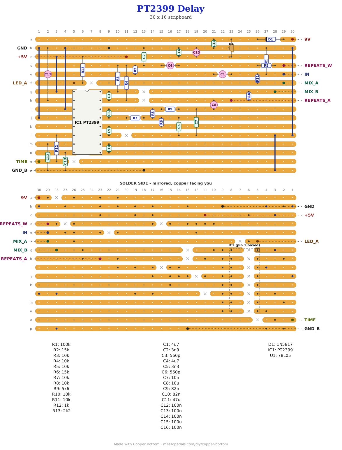
A PT2399 is a whole delay in one chip: an analog-to-digital converter, 44K bits of memory, a converter back, and the clock that sets how long a sound waits in between. Everything outside it is filters and housekeeping, and the datasheet draws all of it. This board is that drawing, value for value, plus the three things a pedal needs that the datasheet leaves out: a regulator so it runs from 9V, a floor under the time knob so the clock cannot be run into the ground, and a mix knob so you can have the repeats without the dry, or the other way round. About 40 milliseconds to half a second, and it gets grittier the longer you make it, which is the charm.
What you'll need
tap to expand / collapse
- 1× PT2399 echo processor, 16-pin DIP - spot it: PT2399 printed on top, notch marks pin 1. Cheap and everywhere; buy two, they are not all good
- 1× 78L05 regulator, TO-92 - spot it: 78L05 on the flat face. The chip is 5V only and will die on 9V
- 1× 1N5817 Schottky - spot it: black body, silver band. Reverse-polarity protection ahead of the regulator
- 7× 10K (brown-black-orange) - the two filters' ins and feedbacks, the repeats path, and the two mix legs
- 2× 15K (brown-green-orange) - the two filters' series inputs
- 1× 5K6 (green-blue-red) on the wet output, 1× 100K (brown-black-yellow) holding the input down, 1× 1K (brown-black-red) under the time pot, 1× 2K2 (red-red-red) for the LED
- 2× 560pF ceramic (561) across the two filter op-amps
- 1× 3.9nF (392) and 1× 3.3nF (332) - the filters' shunt caps. Getting these two backwards moves both corner frequencies a little and nothing else; do not lose sleep
- 2× 82nF (823) - the integrators, one across pins 9 and 10, one across 11 and 12. These set the chip's noise floor; film if you have it
- 1× 10nF (103) on the wet output, 3× 100nF (104) for the clock pins and the regulator, 1× more on the 5V rail
- 2× 4.7 µF electrolytic - input coupling and the repeats path. Spot it: the stripe marks the negative leg
- 1× 10 µF electrolytic on the wet output, 1× 47 µF on the reference pin, 1× 100 µF on the 5V rail
- 1× stripboard, 16 strips × 30 holes or larger, and wire for five links
Off the board
- 1× 50K linear pot (B50K) - TIME. Two lugs
- 1× 50K linear pot (B50K) - REPEATS. All three lugs
- 1× 50K linear pot (B50K) - MIX. All three lugs; the wiper is the output jack
- 1× LED for the panel, any color - power
- 2× 3.5 mm jacks - in and out
- 1× 9V battery snap or a DC jack, and a toggle for power
- An upright 125B - the drill template further down
The layout file is the guide
Like the 555 theremin and the Opto Duet, the build document for this one is the file itself: ↓ Download PT2399_Delay.json - import it into Copper Bottom and the editor gives you the board picture, the placement walkthrough, the electrical checks and a printable build sheet, all from the same file. No coordinates are written out on this page on purpose: the editor is the viewer, and a number typed twice is a number that can drift.
The netlist
Quoted verbatim from the layout file. It was written from the board, so checking the board against it can only pass - what it is for is carrying the circuit somewhere else, and telling you what each strip is supposed to be doing while you stare at it.
The off-board wiring
Eleven pads leave the board. Three pots, two jacks, an LED, and the supply.
| Pad | Goes to |
|---|---|
| 9V / GND | The supply, 9V, through the power toggle. GND also takes both jack sleeves and the LED cathode. GND_B is a second ground pad, the same net, for the pots |
| IN | Input jack tip |
| TIME | The time pot, one outer lug; the other lug to GND_B. Two lugs, a variable resistor. The 1K floor is on the board, so the knob cannot take the chip to zero |
| REPEATS_A / REPEATS_W | The repeats pot. Lug 3 to REPEATS_A, the wiper to REPEATS_W, lug 1 to GND_B. Fully up it will run away, which is a feature |
| MIX_A / MIX_B | The mix pot. Lug 1 to MIX_A (dry), lug 3 to MIX_B (wet), and the wiper goes straight to the output jack tip. There is no OUT pad: the pot is the output |
| LED_A | The power LED's anode. Cathode to GND |
| +5V | Nothing. A test point on the regulated rail, and it tells Copper Bottom's checker that strip is a supply. It is also the first thing to measure if the board is dead: 5V here, or nothing else matters |
The pots are all 50K linear, which is a convenience: one bag. The time pot is the one the datasheet calls R and specifies at 10K to 50K - 50K gives the longest, most degraded delays; a 20K in its place gives a tighter, cleaner range. The mix pot is passive, so at the dry end the wet is not gone, only quiet, and the two do not sum to a constant loudness. That is what a passive blend does; the price of no fourth op-amp.
How it works, in one breath
The signal comes in through a 4.7 µF and a 15K into the first op-amp on the chip, pins 16 and 15, which the 10K, 10K, 560pF and 3.9nF around it make into a second-order low-pass filter - the anti-aliasing filter, cutting everything above a few kilohertz so the converter does not fold it back down as garbage. From pin 15 the chip takes it inside: converts it, walks it through the memory at whatever rate the clock is running, and converts it back through the integrator on pins 11 and 12. The second op-amp on pins 13 and 14 is the same filter again - 15K, 10K, 10K, 560pF, 3.3nF - smoothing the steps back into audio. A 5.6K and 10nF take the last of the clock off it, a 10 µF couples it out, and that is the wet signal.
Time is the resistor on pin 6: it sets the clock, and the clock sets how long a sample waits in memory. The datasheet's table runs from 31 milliseconds at zero ohms to 342 at 27.6K, and the note says 50K is allowed and goes further, with the distortion climbing as it goes - the memory is a fixed size, so a slower clock means fewer samples per second of sound. Repeats takes the wet signal, through the pot and a 10K and a 4.7 µF, back into the input filter's middle node, so what came out goes round again, quieter each time. Mix is dry from the jack and wet from the output, a 10K each, across a pot.
Two things the datasheet says that the page repeats because they bite. The chip wants 5V, from 4.5 to 5.5; that is why there is a 78L05, and why the first measurement on a dead board is the +5V pad. And the 47 µF on pin 2 is the half-supply reference the whole audio path swings around; leave it out and the chip works badly rather than not at all, which is worse.
Unbuilt, and these are the bench numbers. How noisy the long end gets, how hot the 78L05 runs on a wall wart (the chip pulls about 40 mA, which a TO-92 regulator will notice at 12V in), and whether the passive mix has enough level at the wet end into what comes next. If the whine of the clock is audible at short times, the 10nF on the wet output is the one to grow.
Print at 100% / “Actual size”, never “Fit to page” - check the bar measures exactly 4″ before you touch a drill. The face is 66 by 121 mm but only 42 mm of it is drillable once the lid lip is clear.
Nobody has drilled this one yet. The hole sizes come from the parts; where they sit is this format applied to them. Offer the sheet up to the box and check it against your own parts before you make a hole.
Circuit from the PT2399 datasheet's echo application circuit, Princeton Technology, 1998 - every filter value and every housekeeping cap is theirs. The regulator, the time floor, the passive mix, the layout and the box are Onion Madder's, drawn in Copper Bottom.