Ring Mod Booster
One transistor in front of the ring modulator · LPB-1 values on nine strips · By Onion Madder · Mess O' Pedals
The Simple Ring Modulator hears my own synths beautifully, barely hears a circuit-bent toy, and does not hear a guitar at all. That is not the ring being fussy, it is the ring being passive: a diode ring has no gain, and its 600 Ω windings pull a weak, high-impedance source down to almost nothing, so the diodes never open. This board goes in front of the program input and fixes both halves of that. It is the Electro-Harmonix LPB-1, the most-copied one-transistor booster there is, on a nine-by-thirteen scrap with no cuts: it turns a guitar into volts and hands them over from a low impedance. The 100k pot on its output is the level control a diode ring wants anyway - the program has to sit quieter than the carrier, or you hear both inputs bleeding through instead of the sum and difference.
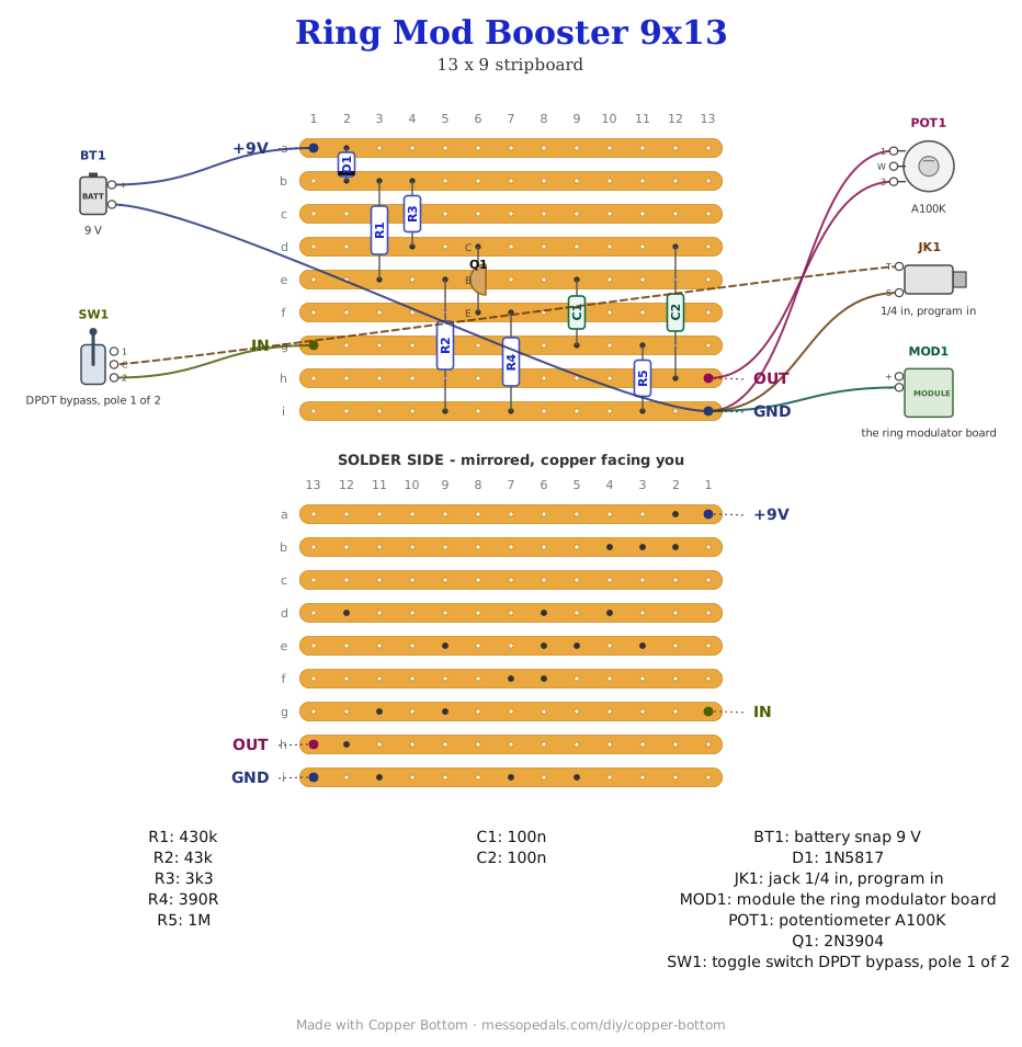
What you'll need
tap to expand / collapse
- 1× 2N3904 NPN transistor (Q1) - spot it: the small black half-round body with the type printed on the flat face. With the flat face toward you and the legs down, the legs are E, B, C left to right. On this board it sits in one column with its three legs across three strips, and the drawing labels each leg
- 1× 1N5817 Schottky (D1) - spot it: small black body, band at the cathode end. Reverse-polarity protection; it stands up, band toward the clean rail
- 1× 430K (yellow-orange-yellow, R1) - from the rail to the base
- 1× 43K (yellow-orange-orange, R2) - from the base to ground. Do not swap these two. 430K up and 43K down puts the base near a volt, which is where the transistor amplifies. The other way round pins the base near the rail and it does nothing but pass DC
- 1× 3K3 (orange-orange-red, R3) - the collector load. Stands up
- 1× 390R (orange-white-brown, R4) - the emitter resistor. The gain is very nearly R3 divided by R4
- 1× 1M (brown-black-green, R5) - the input pull-down. Stands up. It is why the bypass toggle does not pop
- 2× 100n film (104, C1 and C2) - in and out coupling. Ceramic discs work; film is quieter
- 1× stripboard, 9 strips × 13 holes or larger. No cuts, no links: every part stands across strips in its own column
Off the board
- 1× A100K pot, the program level - spot it: A is audio taper, and audio is right for a level control. Lug 3 to OUT, lug 1 to ground, the wiper goes on to the ring
- 1× DPDT on-on toggle, the bypass. One pole switches the jack between straight-through and the booster's input, the other switches the ring's MOD IN between straight-through and the pot. The drawing shows pole 1 only, because pole 2 never touches the board; the wiring table has both. It is one part with six lugs
- 1× 1/4 in jack, the program input. This replaces the jack the ring board's MOD IN pad was wired to
- 1× 9V battery snap, or a DC jack. The ring board has no supply of its own, so this is the only battery in the box
- The ring modulator board itself. Its MOD IN and GND pads are where this board's output ends up
The transistor, from the front
 2N3904, TO-92, flat face toward you, legs down
        _____
       (     )
       |_____|
        | | |
        E B C      emitter  base  collector
The three legs land on three different strips in one column: emitter on the strip that feeds R4, base on the strip R1, R2 and C1 share, collector on the strip R3 and C2 share. The drawing labels each leg where it lands. A transistor in backwards is the classic way a one-transistor booster does nothing, so check the letters against the netlist before you power it.
The layout file is the guide
Like the ring modulator it belongs to, the build document for this one is the file itself: ↓ Download Ring_Mod_Booster.json - import it into Copper Bottom and the editor gives you the board picture, the placement walkthrough, the electrical checks and a printable build sheet, all from the same file. No coordinates are written out on this page on purpose: the editor is the viewer, and a number typed twice is a number that can drift.
The netlist
Quoted verbatim from the layout file. It was written from the board, so checking the board against it can only pass - what it is for is carrying the circuit somewhere else, and telling you what each strip is supposed to be doing while you stare at it.
The off-board wiring
Four pads leave the board. The bypass toggle is the only thing that needs explaining.
| Pad | Goes to |
|---|---|
| +9V | The battery snap's red lead, or the DC jack's center pin. It reaches nothing but the Schottky, so a backwards plug does nothing at all |
| GND | Ground: the battery's black lead, the jack sleeve, lug 1 of the pot, and the ring modulator board's GND pad. One ground for both boards |
| IN | The bypass toggle, pole 1, throw B. Pole 1's common is the program jack's tip |
| OUT | Lug 3 of the A100K pot. The wiper goes to the bypass toggle, pole 2, throw B; pole 2's common is the ring board's MOD IN |
The bypass is one DPDT, two poles, wired as a true bypass. Pole 1's common is the jack tip; pole 2's common is the ring's MOD IN. Jumper the two A throws to each other: in that position the jack goes straight to the ring and this board is out of the path. The B throws are this board's IN pad and the pot's wiper: in that position the signal goes jack, booster, pot, ring. R5, the 1M on the input, is what keeps the flip from popping - without it the input cap floats while the board is bypassed and slams when it is switched back in.
How it works, in one breath
It is a single common-emitter stage, the oldest amplifier there is. R1 and R2 divide the supply down to about 0.8 V on the base, which puts about 0.2 V on the emitter and half a milliamp through the transistor, and leaves the collector resting near 7.5 V with room to swing. The signal comes in through C1 onto the base, and whatever it does to the base voltage, the collector does about 3K3 ÷ 390R, roughly eight times, upside down. That is about 18 dB, and it is what turns a guitar's hundred millivolts into the volt or so a diode ring needs to open. C2 takes the DC off the collector and hands the signal to the pot, which sets how hard the ring is hit. Those are the circuit's numbers; nobody has put a meter on this board yet.
The pot is not decoration. A diode ring wants the program signal quieter than the carrier. Run them level and the diodes never fully switch, and what comes out is a ring-flavored blend of both inputs rather than the sum and difference. Turned down, the pot is how you find the point where the guitar disappears and only the sidebands are left. Turned up, it is a fuzz. Both are worth having.
Things to try
- Boost the carrier instead. Nothing here knows which input it is on. If the carrier is the weak one, move the booster to CAR IN
- Less gain. A bigger R4 lowers it: 1K in place of the 390R is about three times instead of eight, closer to a buffer than a boost, for a source that only needed the impedance fixed. Untested
- Leave the bypass out. Inside a box that only ever sees a guitar, wire the jack straight to IN and the pot straight to MOD IN. One less hole and nothing to pop
- A second one on the toys. The bent toys were the middle case, quiet but not silent. The same board on their input should bring them up to where the synths already sit. Untested
Circuit values from the Electro-Harmonix LPB-1, the one-transistor booster half the pedal world has copied since 1968. The Schottky on the supply, the pull-down on the input, the pot as a program level and the layout are Onion Madder's, drawn in Copper Bottom. There is no drill template: this board lives inside the ring modulator's box and adds one knob and one toggle to its face.