Sound Fuckulator
Paul Stevenson's LM567 noise box, traced off his drawing · By Onion Madder · Mess O' Pedals
The original lives here, published July 2012: Sound Fuckulator on Paul In The Lab. Go and read his, it is three sentences and it is better than mine.
An LM567 tone decoder is a chip built to listen for one frequency and close
a switch when it hears it - touch-tone dialers, remote controls, that sort of thing. Paul
Stevenson pointed one at a guitar instead. It half-hears the note, the switch chatters
against what you are playing, and a 2N2222 stage turns the chattering into
something you can put in a song. His own verdict, in 2012, was that it makes a guitar sound
nasty and horrible
, and he meant it as a recommendation. This page is his board,
traced hole for hole, with the two connections it needs to actually run.
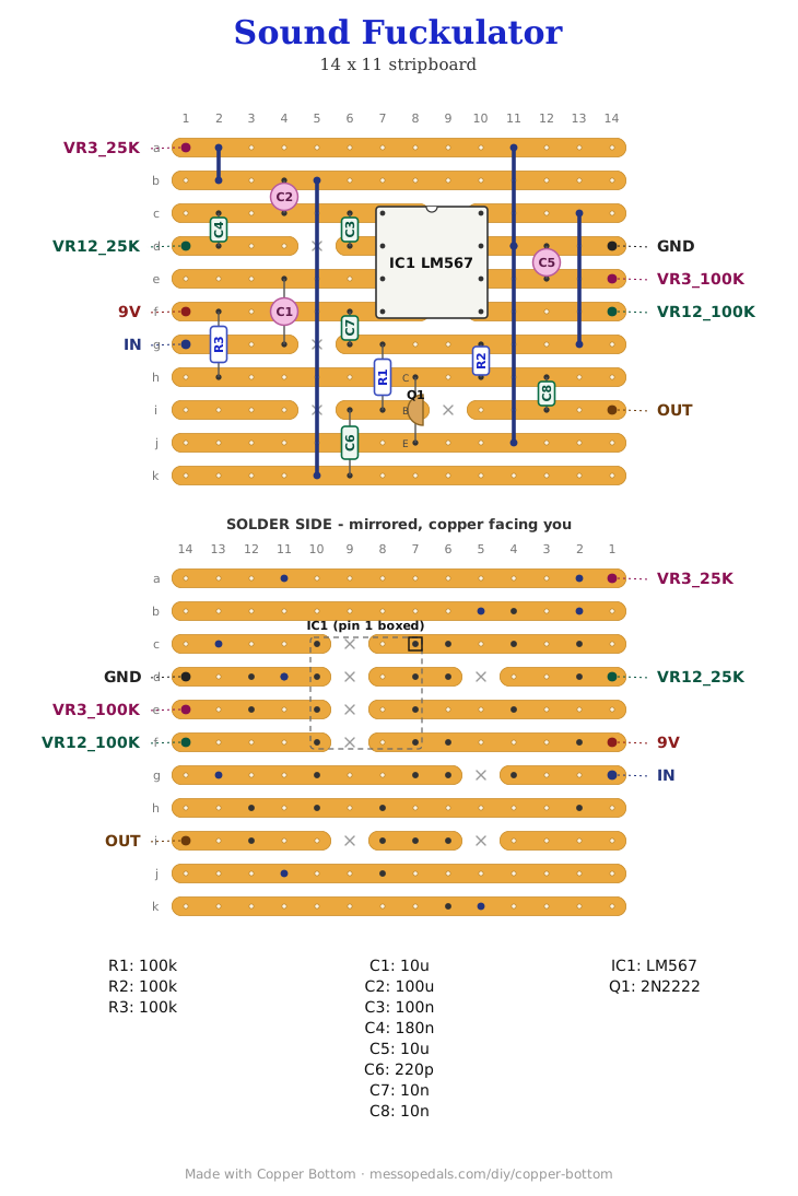
What you'll need
tap to expand / collapse
Fifteen parts on the board, counting the links, and it is a cheap drawer-clearing build. The only thing worth reading twice is the supply, and there is a note about it further down.
- 1× LM567 tone decoder, DIP-8 (IC1) - spot it: eight legs, LM567 or NE567 printed on top, a notch at one end. The NE567 is the same part; so is the LMC567, but that one runs at double the oscillator frequency, so it will not sit where this one does
- 1× 2N2222 NPN transistor (Q1) - spot it: three legs, either a small black half-moon or a little metal can. Check your own part's pinout against the board - the drawing letters the legs C, B and E down strips h, i and j, and the TO-18 metal can and the TO-92 plastic ones are not all lettered the same way round. The board's letters are what to trust
- 3× 100K resistor (R1, R2, R3) - spot it: bands brown-black-yellow. R3 is Q1's collector load, R1 and R2 are the bias pair that also turn out to be the load resistor the chip's output needs
- 2× 10uF electrolytic (C1, C5) - spot it: a little can with a stripe down the minus side. C1 is the input coupling cap, C5 sets the frequency with whatever resistance ends up on pin 5
- 1× 100uF electrolytic (C2) - spot it: the biggest can in the bag. This is the chip's output filter and it wants to be large
- 1× 180nF film capacitor (C4) - spot it: marked 184. An odd value; 150n or 220n will both do something, just not quite the same something
- 1× 100nF film capacitor (C3) - spot it: marked 104. The loop filter, which is what sets how wide a band the chip will answer to
- 2× 10nF ceramic (C7, C8) - spot it: marked 103
- 1× 220pF ceramic (C6) - spot it: marked 221. The smallest cap here and the easiest to grab the wrong one of
- Stripboard, 14 holes by 11 strips, and five wire links
Off the board
- 2× jacks for in and out
- A supply between 3.5V and 8.5V. Paul's pad says 9v. Read the supply note below before you wire a fresh battery to it
- Three pots, VR1, VR2 and VR3, somewhere between 25K and 100K - and this is the part nobody can tell you yet. See the pots
- Wire, and a box if it earns one
The layout file is the guide
Like every layout on this shelf, the build document is the file itself: ↓ Download Sound_Fuckulator.json - import it into Copper Bottom and the editor gives you the board picture, the placement walkthrough, the electrical checks and a printable build sheet, all from the same file. No coordinates are written out on this page on purpose: the editor is the viewer, and a number typed twice is a number that can drift.
There is a second file, and it is there for honesty rather than for building:
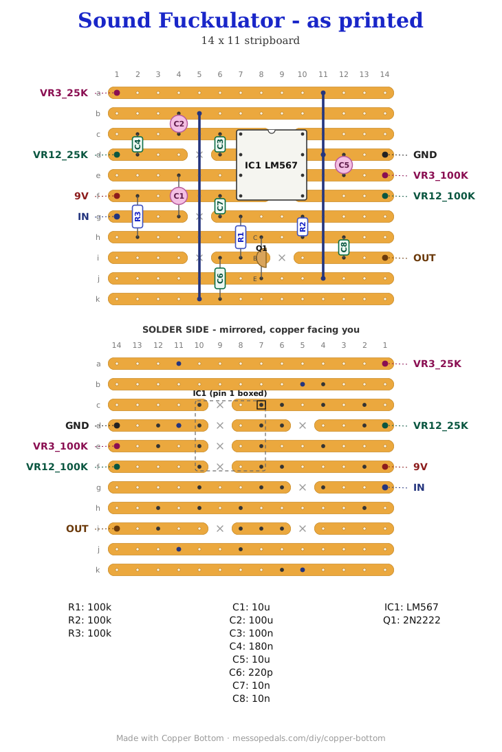
↓ Download Sound_Fuckulator_AsPrinted.json
is Paul's drawing transcribed with nothing added, so you can see exactly what was
published and judge the two additions for yourself. Import it and Copper Bottom will tell you
the same thing it told me: IC1.8 is the only thing on its net - connects nowhere.
If you would rather just look at it than import it, here is the same file drawn out:
↗ Paul's board as printed, drawn.
The two links, and why
Paul drew this straight onto stripboard in 2012 and was upfront that there was never a
schematic behind it - asked for one in the comments two years later, he said he
made this from my head
and had not bothered. So the drawing is the whole document, and
when the drawing is the whole document a missing wire has nowhere to hide. Two nets on his
board have no way of reaching the rest of it.
Neither can be fixed off the board, which is what makes this a certainty rather than an opinion: neither net carries a pad. No pot, jack or flying lead can land on them however the pots turn out to be wired. The only thing that can reach them is a link on the board. Both have been added and nothing else was moved.
- J4, column 13, strip c to strip g. The chip's output had nowhere to go. Pin 8 sat alone on its own stub of strip c. It is an open-collector output, which means it can only pull down and needs a resistor pulling it up - TI's datasheet says in as many words that it requires an external load resistor. Meanwhile the node at strip g - R1 to the transistor's base, R2 to its collector, C7 to the rail - is a textbook bias network with nothing driving it. Land pin 8 on strip g and both problems answer each other: the output gets its 200K pull-up through R2 and R3, and the transistor gets something to react to
- J5, column 2, strip a to strip b. The b and k rail is ground. C2 hangs off pin 1, the output filter, and that cap has to go to ground. C3 is daisy-chained from pin 2 across to pin 1 rather than run to the rail, which works only because a 100uF holds pin 1 at ground as far as any audio signal is concerned - and the datasheet's own rule, that the output filter should be at least twice the loop filter, fits Paul's 100uF against 100nF exactly. C6 then becomes a plain rolloff from the transistor's base to ground. Three separate parts want that rail to be earth, and his drawing never joins it to the earth he already has
None of this is a criticism of the drawing and it should not be read as one. A layout drawn from the head, published free, and left up for fourteen years is a generous thing to do, and the circuit underneath it is his. Two wires is a remarkably short list. If it turns out he wired those two nets some other way on the board he actually built, his answer wins and this page changes.
The pots, which nobody has settled
Paul labels four rows of the board for pots: VR3 25k on the ground rail and VR3 100k on pin 6, VR1,2 25k on C4's far end and VR1,2 100k on pin 5. Three pots, four labels, and each pot name paired with two different numbers. Those numbers could be alternative values, they could mark which lug goes where, or they could be a stated range. The drawing does not say, there is no schematic to check it against, and guessing on your behalf is how somebody ends up wiring a pot across a timing node and wondering why it does nothing.
So the pads are drawn where he put them and named the way he named them, and this page does not pretend to know. What it can give you is one hard constraint to start from.
Pin 5 carries nothing but its pad. Pin 5 is the timing resistor pin and pin
6 is the timing capacitor pin, and the free-running frequency is
fo = 1 / (1.1 × R × C) with that R running from pin 5 to pin 6. C5,
10uF, is already sitting on pin 6. There is no fixed resistor anywhere on pin 5 - so whatever
VR1,2 turns out to be, it has to be what completes that path, or the oscillator has no
timing resistance at all and the chip will not run. Wiring VR1,2 as a variable resistor from
pin 5 to pin 6 is the reading that definitely oscillates, and with 10uF on pin 6 it will land
very low. That last sentence is mine, not his, and it is untested.
The supply, before you plug anything in
The pad says 9v and the LM567's absolute maximum is 9V. TI puts the recommended supply at 3.5V to 8.5V and the absolute maximum - the number past which damage may occur - at 9V flat. A fresh alkaline block sits at 9.5 to 9.6V, and there is no regulator and no series diode anywhere on this board. Paul built his and it worked, so this is margin rather than a wall. Two ordinary silicon diodes in series with the incoming positive drop about 1.4V, land you near 8.2V off a fresh cell, and give you reverse-polarity protection for nothing. The 9V and the 3.5-8.5V are the datasheet; the two diodes are a suggestion.
The netlist
Quoted verbatim from the layout file. It was written from the board, so checking the board against it can only pass - what it is for is carrying the circuit somewhere else, and telling you what each strip is supposed to be doing while you stare at it.
How the chip sits is not a judgement call. Paul drew the pin 1 marker at the top left, but you do not have to take that on trust: pin 4 is the supply pin and it lands on the strip carrying the 9v pad, and pin 7 is ground and it lands on the strip carrying the GND pad. Only one orientation does both. If your DIP goes in the other way round you will find out immediately and expensively.
The off-board wiring
Eight pads leave the board: two jacks, the supply and the four pot connections.
| Pad | Goes to |
|---|---|
| IN | Input jack tip. The sleeve goes to GND. It reaches pin 3 through C1 |
| OUT | Output jack tip. The sleeve goes to GND. It comes off Q1's collector through C8 |
| 9V / GND | The supply, positive to 9V and negative to GND. Read the supply note above first - the chip's absolute maximum is 9V and a fresh battery is over it |
| VR12_100K | Pin 5, the timing resistor pin, and nothing else is on it. Paul marks this one for VR1 and VR2 at 100k |
| VR12_25K | Paul marks this one for VR1 and VR2 at 25k. It reaches pin 1 through C4, so whatever lands here is coupled into the output filter rather than connected to it |
| VR3_100K | Pin 6, the timing capacitor pin, where C5 10uF already sits. Paul marks this one for VR3 at 100k |
| VR3_25K | Paul marks this one for VR3 at 25k. This strip is the ground rail, which is worth knowing before you wire a pot to it |
How it works, in one breath
The LM567 is a phase-locked loop with a detector bolted on. Its oscillator free-runs at
whatever R on pin 5 and C on pin 6 tell it to, your guitar arrives
at pin 3 through C1, and when the two are close enough the loop locks and pin 8 pulls down.
C3 on pin 2 sets how close is close enough; C2 on pin 1 decides how quickly the output is
allowed to change its mind. Feed it a guitar rather than a dial tone and it spends its whole
life half-locking, losing it and grabbing again, which is the sound.
Pin 8 can only pull down, so it hangs on the bias node of the transistor stage - R1 to Q1's base, R2 up to its collector, R3 from the collector to the supply, C7 holding the middle of that divider steady. Q1 is an ordinary common-emitter amplifier with collector-feedback bias, and the chip yanking on its bias is what turns a lock-and-slip into a gated, spitting output. It leaves through C8.
Everything in those two paragraphs is read off the datasheet and off the copper, not off a bench. Nobody here has heard it. The one first-hand account of what it sounds like is Paul's, and he only ever said it was nasty.
Things to try
- Settle the pots. The most useful thing anybody can do with this board is find out what the three controls actually are. Start from pin 5 to pin 6 for VR1,2 and work outward
- Drop C5. 10uF on the timing pin puts the free-running frequency absurdly low. If it will not chatter, a smaller cap there moves the whole thing into the range a guitar actually occupies - 100nF is the datasheet's own typical value, and that is a factor of a hundred
- Feed it something that is not a guitar. A tone decoder pointed at a drum machine, or at another oscillator, is a different instrument. The Dragonfly VCO makes a clean square that this thing should lock to properly, which means you can hear the difference between locking and failing to
- No drill template here, on purpose. Every other boxed layout on this shelf gets a 125B sheet drawn from its own pad list. This one cannot have an honest sheet until somebody knows how many holes the pots need and what to letter them
The circuit and the original layout are Paul Stevenson's, published on Paul In The Lab in July 2012 and free to build ever since. The same hands drew the Devil's Triangle, which is also on this shelf and has been built here twice. What is mine is the trace, the two added links, the checking and the words. The name is his and it stays.