Analog Bit Crusher Mk II
The rate knob put in series, where it works · By Onion Madder · Mess O' Pedals
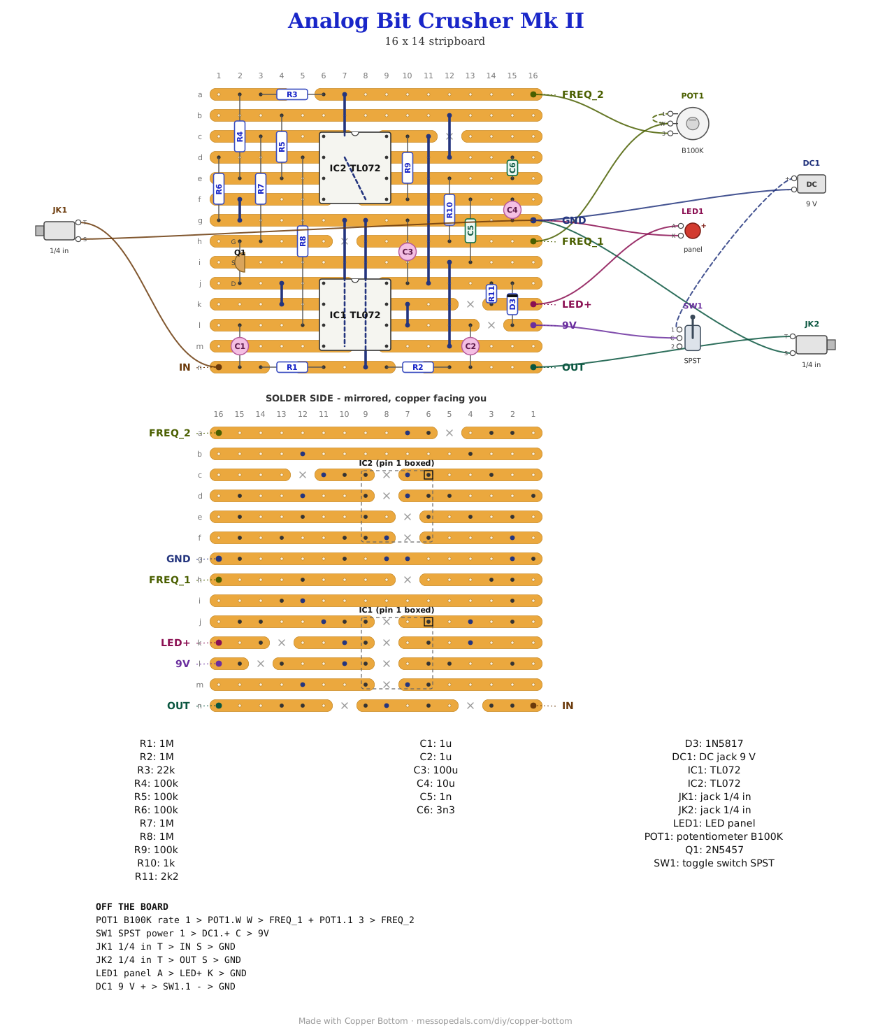
Same crusher as the first board: it crushes the sample rate and not the bit depth, takes a snapshot of the signal, holds it flat until the next one, and the knob decides how often that happens. What is different is the knob. On the first board the rate pot sits outboard of two steering diodes, and one of those diodes ties the clock output straight to the pot's own pad - so half of every cycle bypasses the knob entirely. Here the two diodes come out and the pot sits in series with R10 between the comparator output and the integrator input, which is the plain triangle oscillator and sweeps both halves together. Three holes different, and one resistor value.
What you'll need
tap to expand / collapse
Thirty-one parts on the board and five off it. Nothing here is exotic; the JFET is the only part worth buying carefully.
- 2× dual op-amp, DIP-8 (IC1, IC2) - spot it: eight legs, the number printed on top, a notch at one end. Fit sockets and read the op-amp note below before you pick these. A TL072 in IC1 and an NE5532 in IC2 is the pair that three separate people got working; two TL072s is the combination that gives a clean signal and no crushing at all
- 1× 2N5457 N-channel JFET (Q1) - spot it: TO-92, three legs, one flat face, 2N5457 on the flat. This is the sampler. A J201 or a 2N5458 works. It is not a 2N3904 and a 2N3904 will not do anything useful here
- 4× 1M resistor (R1, R2, R7, R8) - spot it: bands brown-black-green. Two hold the jacks at ground, one biases the input, and R7 is the one that lets the clock drive the JFET's gate without loading it
- 4× 100K resistor (R4, R5, R6, R9) - spot it: bands brown-black-yellow. Two make the half-supply reference, two set how far the clock swings
- 1× 22K resistor (R3) - spot it: bands red-red-orange. It sits in series with R4, and the pair of them is deliberate - see the netlist note
- 1× 1K resistor (R10) - spot it: bands brown-black-red. Colin's layout has 100R here and this board has 1K. R10 is what the clock op-amp has to drive, and 100 ohms is more than a TL072 can pull; 1K is comfortable and still puts the fast end of the knob well above hearing. It is also the floor under the pot, so the knob needs no resistor of its own
- 1× 2K2 resistor (R11) - spot it: bands red-red-red. The LED's series resistor, and the only part on the board that does nothing for the sound
- 2× 1 µF electrolytic (C1, C2) - spot it: a small can with a stripe down one side. In and out coupling; the stripe faces the jack on both of them
- 1× 10 µF electrolytic (C4) - decouples the half-supply reference. Stripe to ground
- 1× 100 µF electrolytic (C3) - the supply reservoir. Stripe to ground
- 1× 1nF film or ceramic (C5) - spot it: printed 102. This is the memory. Use film if you have it: a cheap ceramic leaks and droops, and droop here is the sound sagging between samples
- 1× 3n3 film or ceramic (C6) - spot it: printed 332. The clock's timing cap, and the part to change if you want a different range of sample rates
- 1× 1N5817 Schottky (D3) - spot it: fatter black body, band at one end. Reverse-polarity protection on the supply. It stands on end - see the note under the layout file
- 10× wire links (J1 to J10) - offcuts of component leg. J10 is the one diagonal, under IC2
Off the board
- 1× B100K linear pot - the rate knob. Wired as a variable resistor: wiper tied to one outer lug, that pair to FREQ_1, the remaining lug to FREQ_2. R10 on the board is its floor, so this one needs no extra resistor in series. Colin specifies 1M or 2M and 100K is my call - builders of the original agreed the top of a 1M is unusable, and 100K puts the whole rotation inside the part that does something
- 1× LED and nothing else - anode to LED+, cathode to ground. R11 is already on the board
- 2× 1/4″ jacks - in and out. 3.5 mm works just as well if this is going in a synth box rather than on a pedalboard; nothing in the circuit cares
- 1× DC jack, 9 V, center negative or center positive as you like - D3 means a backwards plug does nothing at all
- No bypass and no footswitch. There is none in the layout file, so there is none on the drill template either. It is always on; wire a true-bypass loop around it if you want one
- An SPST toggle for power, in the positive supply lead between the DC jack or battery and the board's supply pad. Not in the layout file - it is off the board, and every build on this shelf gets one
The layout file is the guide
Like every layout on this shelf, the build document for this one is the file itself: ↓ Download Analog_Bit_Crusher_MkII.json - import it into Copper Bottom and the editor gives you the board picture, the placement walkthrough, the electrical checks and a printable build sheet, all from the same file. No coordinates are written out on this page on purpose: the editor is the viewer, and a number typed twice is a number that can drift.
Two parts stand on end, and that is deliberate. D3, the 1N5817, has two strips to cross and a DO-41 body is longer than that, so it stands up rather than lying flat. R11 does the same between its two strips. Standing an axial part up is ordinary and it works; all it changes is how tall the finished board is, which is what catches you when the lid goes on.
The netlist
Quoted verbatim from the layout file, and emitted from the copper rather than typed
beside it - so checking the board against it can only pass. What it is for is carrying the
circuit somewhere else, and telling you what each strip is doing while you stare at it. The
line worth finding is IC2_OUTA: the FREQ_2 pad is on it now, which is the whole
difference between this board and the first one.
R3_A is a net with nothing on it but two resistor legs, and it is not a
mistake. R3 (22K) and R4 (100K) sit end to end, so what the clock actually sees is
122K. Two parts where one would do, because 122K is the number the hysteresis wants and 122K
is not a value you can buy. If you would rather fit one resistor, 120K goes in R4's holes
with a link where R3 was.
The off-board wiring
Seven pads leave the board: one knob, one LED, two jacks and the supply.
| Pad | Goes to |
|---|---|
| IN | Input jack tip. The sleeve goes to GND |
| OUT | Output jack tip. The sleeve goes to GND |
| FREQ_1 / FREQ_2 | The rate pot, B100K. Tie the wiper to one outer lug and run that pair to FREQ_1; the remaining outer lug goes to FREQ_2. A variable resistor, not a divider - and unlike the pitch pots on the Cicada NAND it needs no resistor of its own in series, because R10 on the board is already doing that job. Both pads moved relative to the first board: FREQ_2 is now on the top strip, on the clock chip's own output, so the pot sits in the current path rather than off to one side of it |
| LED+ | LED anode. The cathode goes to GND. R11 is on the board, so the LED wires straight to the pad |
| 9V / GND | The supply. DC jack positive to 9V, negative to GND, and GND is also both jack sleeves and the LED cathode. D3 is already in the way of a backwards plug |
How it works, in one breath
The signal comes in through C1, gets biased to half the supply by R8, and lands on the first half of IC1 wired as a follower - output tied straight back to its own inverting input, so it copies the signal and drives the JFET without loading anything. Q1 is the switch. Its drain sees that copy; its source sits on C5, the 1nF. When the clock pulls Q1's gate up, the JFET conducts and C5 charges to whatever the signal is doing at that instant. When the gate goes back down the JFET turns off and C5 is left holding that voltage, with nowhere to leak to: the second half of IC1 is another follower and a TL072's input draws essentially nothing. That held voltage leaves through C2. So the output is the input, redrawn as a staircase, and the width of each step is the whole effect.
IC2 is what sets that width, and it is the oldest trick in the op-amp book: a comparator and an integrator chasing each other. The second half integrates - C6 across it, current in through R10 - so its output ramps. The first half watches that ramp against the half-supply reference through R5 and the R3 plus R4 pair, and flips its output the moment the ramp goes far enough. The flip reverses the current into the integrator, so the ramp turns round, and round it goes. The knob is simply in the way of that current. It sits in series with R10 between the comparator output and the integrator input, so winding it up lengthens both halves of the cycle equally and the clock slows down. Colin's board puts a pair of steering diodes between the two, and one of them hands the charging current a short cut through R10 on its own - which means half of every cycle never sees the knob at all. Taking the diodes out is the whole change.
The arithmetic, and it is arithmetic and not a measurement. With C6 at 3n3 and the pot wide open at 100K, the period works out near 1 ms, so the sample clock lands around 900 Hz - a heavy crush, roughly a telephone made of gravel. With the pot at zero the only thing left in the path is R10 at 1K, which puts the clock near 90 kHz: well above hearing, so that end of the travel is the effect switched off. The sweep is even now, which it was not before - with the diodes in, one half-cycle stayed fast whatever you did, so the duty cycle went lopsided instead of the rate coming down, and the sampling window got narrow enough that C5 had trouble charging through the JFET at all.
The op-amp, which is the part that decides whether this works
This circuit is famously fussy about which chips go in it, and the reports are consistent enough to build around. Three people who built Colin's layout say the same thing: two TL072s give a clean signal and no crushing at all. The cure they converge on is a bipolar-input op-amp in IC2, the clock - an NE5532, or a 4558, 1458 or LM358 - with a TL072 perfectly happy in IC1. fuzzhead, who posted the layout, says the same. The layout's own note just says to try several.
There is a reason that fits. R10 is the load the clock op-amp drives, and at Colin's 100R a TL072 simply cannot pull it; an NE5532 is built to drive low impedances. R10 is 1K on this board partly for that reason, so it is possible that two TL072s now work here where they did not before. That is a guess and it is the interesting experiment this board is for: socket both chips, start with the NE5532 in IC2 because that is the combination known to work, and then try a TL072 in it and see.
The whine is part of the circuit, not your build. Every builder reports the oscillator bleeding through, audible even in bypass, and nobody has solved it. If you want this effect without that, Parasit Studio's Sonic Reducer is the same idea done properly and there is a layout for it on the same site.
Things to try
None of these have been tried, because none of this has. They are the obvious knobs.
- Put the diodes back, deliberately. With the pot in series the way it is now, adding a diode and a second resistor across it would give you a real duty-cycle control instead of the accidental one Colin's board has. That is a different knob, not a fix, and it wants its own pads.
- Change C6. It sets the whole range. 10n takes the slow end down to a few hundred hertz, which stops being a crusher and starts being a ring modulator with delusions; 1n moves the useful part of the sweep up where it is gentler.
- Put a pot in series with R7. The gate drive decides how hard the JFET switches, and softening it blurs the edge of each step rather than the rate.
- Take the clock out to a jack. IC2 pin 1 is a square wave with the rate on a knob and nothing else using it. That is a usable LFO or gate for anything else in the box.
- Feed the clock from somewhere else. Lift R7 from IC2 pin 1 and drive it from another oscillator instead, and the crush follows whatever that is doing.
- A wet/dry blend. The dry signal is already buffered at IC1 pin 1. A pot between there and the output, against C2, mixes the staircase back under the real thing.
The DC jack is not on the sheet - it goes on a wall. Two 1/4″ jacks and a barrel will not sit inside the lid lip: a jack wants 16 mm of room and the barrel 12, and there are only 42 mm of face to share between them.
↓ Or with the jacks on top
Print at 100% / “Actual size”, never “Fit to page” - check the bar measures exactly what it says before you touch a drill. The dashed line is the keep-out for the lid lip and the corner bosses.
Nobody has drilled this one yet. The hole sizes come from the parts the layout file names; where they sit is this format applied to them. Offer the sheet up to your own box and your own parts before you make a hole.
The sample-and-hold is as old as the JFET and belongs to nobody - it is the front half of every analog-to-digital converter ever made, used here without the digital half. The comparator-and-integrator clock is the same. The circuit came off the Experimentalist Anonymous forum, and the stripboard layout this one is derived from is Colin Reaffels', published by fuzzhead at Dirtbox Layouts in February 2022, along with the builder reports that the op-amp note above is built on. The first board is his hole for hole. This one is not: the two steering diodes are gone, the FREQ_2 pad has moved onto the comparator output, R10 is 1K where he has 100R, there is one extra cut to keep the indicator LED off the sample-and-hold node, and the pot is 100K where he calls for 1M or 2M. Those are mine and so is anything wrong with them. IvIark laid the same circuit out differently at Tagboard Effects in 2012 if you want to compare.