ISD1820 on a Breadboard
A bare-chip sampler, one voice · By Onion Madder · Mess O' Pedals
Level: Advanced - what the levels mean
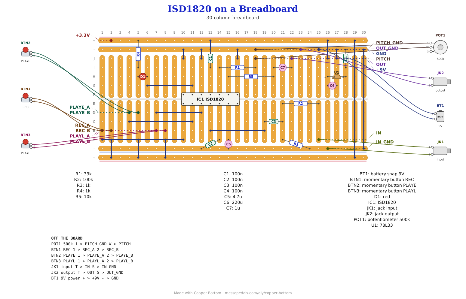
The ISD1820 usually arrives already soldered to a little red module with a microphone and three buttons on it. This build skips the module and puts the bare chip on a breadboard, so every part around it is one you chose and can change: a line input instead of the microphone, three buttons, a record LED, and a 3.3V regulator so it runs from a 9V battery.
It goes together in three stages. First it is a plain recorder with a speaker clipped on, which proves the chip and the wiring. Then one resistor comes out and a pitch knob goes in. Last, the speaker comes off and a line out takes its place. Each stage is a few parts, and the board works at the end of every one.
If you would rather start from the module, the ISD1820 Breakout guide wires one up with all four of its modes.
⚠ Before you start tap to expand / collapse
The 9V never touches a rail. The battery's red lead goes to one hole, J28, which is the regulator's input. Both + rails carry 3.3V from the regulator's output. The ISD1820 is rated for 2.4V to 5.5V, so 9V on a + rail would be the end of it.
The regulator's leg order is the 78L33's, and other 3.3V parts in the same package differ. With the flat face toward you and the legs down, a 78L33 reads OUT, GND, IN from left to right. Read the marking on yours before it goes in. A different regulator needs its own datasheet.
Four parts care which way around they go. The three electrolytics each have a stripe down one side marking the minus leg, and the LED has a short leg and a flat on its rim marking the cathode. The steps name the hole for each leg.
Meter your rails before you wire anything. This layout runs from column 1 to column 28. If your board's rails are split partway along, bridge each half with a jumper first. A split rail is the single most common reason a breadboard build does nothing at all.
Leave the battery off until step 35, and unclip it again before each of the two later stages.
What you'll need
tap to expand / collapse
The parts list lives on the build sheet too - this version adds how to spot each part in a drawer.
- 1× ISD1820 record and playback chip, DIP-14 - spot it: fourteen legs, ISD1820 printed on top, a notch at one end. The same chip that sits on the red voice recorder modules, here on its own
- 1× 78L33 3.3V regulator, TO-92 - spot it: a small black half-cylinder with three legs, the size of a transistor, marked 78L33 on its flat face. Read the marking: it looks exactly like a transistor
- 1× LED, any color - spot it: the short leg and the flat on the rim are the cathode. It lights while the chip is recording
- 2× 1K resistor - spot it: bands brown-black-red. One for the LED, one for the bottom of the input divider
- 2× 100K resistor - spot it: bands brown-black-yellow. One for the top of the input divider, and one that sets the chip's clock. The clock one comes back out at step 39
- 1× 33K resistor - spot it: bands orange-orange-orange. Not needed until the pitch knob goes in at step 40
- 1× 10K resistor - spot it: bands brown-black-orange. Not needed until the line out at step 44
- 4× 100nF ceramic - spot it: disc printed 104. Either way around
- 1× 4.7 µF electrolytic - spot it: a small can with a stripe down one side marking the minus leg
- 1× 220 µF electrolytic - spot it: the big can. It sits across the regulator's output
- 1× 1 µF electrolytic - spot it: the smallest can. Not needed until the line out at step 45
- 1× 500K pot - the pitch knob. Not needed until step 41. Two of its three lugs are used
- 3× momentary push button - REC, PLAYE and PLAYL. Each one sits across two neighboring columns, so it needs two legs that will reach holes one apart. A button with wire tails soldered on does it
- 1× input jack - whatever your phone or source plugs into, with two leads on it
- 1× output jack - whatever your amp or mixer takes. Not needed until step 46
- 1× 8 ohm speaker with two leads or clip leads - for the first test only. It comes off again at step 43
- A breadboard with both banks, both rail pairs and at least 30 columns - spot it: a half-size board is enough. Plus sixteen jumpers at the start and one more for the bend
- 9V battery and a snap
- 1× multimeter - any cheap one that reads ohms and DC volts. It checks each rail end to end before you wire anything, and the 3.3V at step 35
Reading the breadboard
This guide names exact holes, like E10 or J28. Letters run across the board and numbers run along it, and both are printed on the board itself, so every instruction below points at one hole you can put a finger on.
The center channel splits the letters into two banks: A to E on one side and F to J on the other, with E and F being the two rows either side of the channel. The five holes in a bank that share a number are all the same electrical point, which is why a step sometimes names a different row than you would expect - any free hole in that column and bank will do.
Turn the board so the numbers climb left to right. Then A to E is the lower bank and F to J the upper bank, the top rails are the pair above F to J and the bottom rails are the pair below A to E. This build uses both banks and both rail pairs. Before you wire anything, meter each rail end to end; if yours is split, bridge each half with a jumper first.
The same column number is two different points. Column 5 in the lower bank is a button and column 5 in the upper bank is the LED, and the center channel keeps them apart. The same goes for columns 6, 13, 14, 15 and 16. Read the letter as well as the number.
Quick reference - the whole build on one card
The pinout with the hole every pin lands in. The steps below walk through it slowly; this is the bench card.
The notch points left and pin 1 goes in E10, so pin 14 lands in F10 directly across the channel. Then every other pin falls on the hole shown. Anywhere in the same bank and column is the same point, so F14 and I14 are both “pin 10”. RLED is the pin the datasheet calls RECLED and MREF is MICREF.
Power
- 78L33, flat toward you: OUT H26, GND H27, IN H28
- J26 → top +; J27 → top −; 9V red → J28, black → top −
- 220µF: + G26, − G27. 100nF: I28 → top −
- Bridge + → + and − → − between the top and bottom rail pairs
- Both + rails are 3.3V. The 9V only ever reaches J28
The chip's upper side
- J10, J12 and J16 → top − (VSSD, FT, VSSA)
- J13 → top + (VCC); 100nF: I13 → top −
- 100K: I14 → top − (ROSC)
- G11 → G6; LED cathode H6, anode H5; 1K: I5 → top +
The input
- 4.7µF: + A15, − bottom − (AGC)
- 100nF: A14 → bottom − (MICREF)
- B13 → B19; 100nF: C19 → C21; 1K: A21 → bottom −
- 100K: E21 → E25; jack tip → A25, sleeve → bottom −
The buttons
- REC: A10 → A1, button B1 to B2, A2 → bottom +
- PLAYE: C11 → C4, button D4 to D5, A5 → bottom +
- PLAYL: D12 → D7, button B7 to B8, A8 → bottom +
Steps 1–3 The chip, the regulator and the LED
The chip goes in dry, before a single wire. Every other part on the board is measured from its footprint.
| Step | Do |
|---|---|
| 1 | Seat the ISD1820 across the center channel, notch to the left: pin 1 in E10, pin 7 in E16, pin 8 in F16, pin 14 in F10. Pins 1 to 7 land in E10 to E16 and pins 14 down to 8 land in F10 to F16. Press it flat and check no leg folded under |
| 2 | Place the 78L33 with its flat face toward you: OUT in H26, GND in H27, IN in H28 |
| 3 | Place the LED: cathode in H6, the short leg, and anode in H5 |
Steps 4–19 The jumpers
Sixteen wires. Do the two rail ties first: the buttons take their 3.3V from the bottom + rail and the regulator feeds the top one, so nothing in the lower bank has power until the pairs are joined.
| Step | Do |
|---|---|
| 4 | Bottom − rail to top − rail. Ties the two negative rails together |
| 5 | Bottom + rail to top + rail. Ties the two positive rails together |
| 6 | J10 to the top − rail. This is pin 14, VSSD, the chip's digital ground |
| 7 | J16 to the top − rail. Pin 8, VSSA, the analog ground |
| 8 | J13 to the top + rail. Pin 11, VCC, the chip's supply |
| 9 | J12 to the top − rail. Pin 12, FT. Held low, feed-through is off |
| 10 | J26 to the top + rail. The regulator's output, and the only thing that feeds the + rails |
| 11 | J27 to the top − rail. The regulator's ground |
| 12 | G11 to G6. Carries pin 13, RECLED, over to the LED's cathode |
| 13 | B13 to B19. Carries pin 4, MIC, out to where the input parts sit |
| 14 | A10 to A1. Pin 1, REC, out to its button |
| 15 | A2 to the bottom + rail. The other side of the REC button |
| 16 | C11 to C4. Pin 2, PLAYE, out to its button |
| 17 | A5 to the bottom + rail. The other side of the PLAYE button |
| 18 | D12 to D7. Pin 3, PLAYL, out to its button |
| 19 | A8 to the bottom + rail. The other side of the PLAYL button |
Steps 20–23 The resistors
Two values, two of each. The 1K and the 100K differ only in the third band, red against yellow.
| Step | Do |
|---|---|
| 20 | 100K (brown-black-yellow): I14 to the top − rail. Pin 10, ROSC. This resistor sets the chip's clock, and it is the one that comes out again at step 39 |
| 21 | 100K: E21 to E25. The top of the input divider. Column 25 is the input jack's tip |
| 22 | 1K (brown-black-red): A21 to the bottom − rail. The bottom of the input divider |
| 23 | 1K: I5 to the top + rail. The LED's resistor, on its anode |
Steps 24–27 The ceramic caps
Four of the same part, printed 104, and none of them care which way around they go.
| Step | Do |
|---|---|
| 24 | 100nF: I13 to the top − rail. Supply decoupling, right at the chip's VCC pin |
| 25 | 100nF: A14 to the bottom − rail. Pin 5, MICREF |
| 26 | 100nF: C19 to C21. The input coupling cap. Column 21 is now the input node |
| 27 | 100nF: I28 to the top − rail. Across the regulator's input |
Steps 28–29 The electrolytics
Both have a direction. The stripe marks the minus leg.
| Step | Do |
|---|---|
| 28 | 4.7 µF: plus leg in A15, pin 6, AGC, and the stripe leg in the bottom − rail |
| 29 | 220 µF: plus leg in G26, the regulator's output, and the stripe leg in G27, its ground |
Steps 30–35 The buttons, the input jack and power
Each button bridges two neighboring columns. One column already runs to a chip pin and the other to the + rail, from the jumpers at steps 14 to 19.
| Step | Do |
|---|---|
| 30 | The REC button across B1 and B2 |
| 31 | The PLAYE button across D4 and D5 |
| 32 | The PLAYL button across B7 and B8 |
| 33 | Input jack tip to A25 |
| 34 | Input jack sleeve to the bottom − rail |
| 35 | The 9V snap: red to J28, black to the top − rail. Before you clip the battery on, check the chip's notch points left, the regulator's flat faces you, and the red lead is in J28 and not in a rail. Clip it on and meter the top + rail against the top − rail: it should read close to 3.3V. Anything near 9V means the regulator is in backwards; unclip the battery straight away |
Steps 36–38 First test, module-style
With a speaker clipped straight across the chip's two speaker pins, this is the same circuit as a stock recorder module with a jack where its microphone would be.
| Step | Do |
|---|---|
| 36 | Clip the 8 ohm speaker between A16, pin 7, SP−, and I15, pin 9, SP+ |
| 37 | Plug a phone into the input jack, hold REC and play some audio. The LED should light for as long as you hold it |
| 38 | Release REC and tap PLAYE. It should play the recording back like a stock module |
Steps 39–42 The bend: a pitch knob
Unclip the battery first. The 100K on ROSC sets how fast the chip clocks its memory. Swap it for a 33K with a 500K pot behind it and the knob is the pitch.
Untested. Nobody has turned this knob yet. The 33K is there so the pot at zero still leaves some resistance on the pin.
| Step | Do |
|---|---|
| 39 | Pull the 100K from step 20, the one from I14 to the top − rail |
| 40 | 33K (orange-orange-orange): I14 to I18 |
| 41 | The 500K pot's wiper to J18 |
| 42 | One outer pot lug to the top − rail. The third lug stays empty |
Steps 43–47 The line out
Unclip the battery first. The speaker comes off and a jack goes on in its place, fed from one of the two speaker pins.
Untested. Nobody has plugged this output into anything yet. Start with the amp or mixer turned down.
| Step | Do |
|---|---|
| 43 | Remove the speaker |
| 44 | 10K (brown-black-orange): H15, pin 9, SP+, to H20 |
| 45 | 1 µF electrolytic: plus leg in I20 and the stripe leg in I22 |
| 46 | Output jack tip to J22 |
| 47 | Output jack sleeve to the top − rail. Leave SP−, pin 7, with nothing on it |
⚠ If it doesn't work
| Symptom | Check |
|---|---|
| Nothing at all, and no 3.3V on the rails. | The regulator. Flat face toward you, OUT in H26, GND in H27, IN in H28, the red battery lead in J28, and the two jumpers from J26 and J27 reaching the top rails. Then a flat battery. |
| 3.3V on the top rails but not the bottom ones. | The two rail ties, or a rail that is split partway along the board. |
| 3.3V everywhere and the chip does nothing. | The chip's own four connections: J13 to +, and J10, J16 and J12 to −. Then the notch pointing left, and a folded leg under the body. |
| The LED does not light while REC is held. | The LED the wrong way around: cathode in H6, anode in H5. Then the 1K from I5 to the top + rail, the jumper from G11 to G6, and the REC button actually bridging B1 and B2 with A2 reaching the + rail. |
| The LED lights but the recording is silent. | The input chain, in order: jack tip in A25, the 100K from E25 to E21, the 100nF from C21 to C19, the jumper from B19 to B13. Then the source itself: turn the phone up. |
| The recording is there but very quiet. | The divider cuts the input down a long way on purpose, to microphone level. Turn the source up first. The 4.7 µF on A15 in backwards is the other suspect. |
| It records, and PLAYE does nothing. | That button: the jumper from C11 to C4, the button across D4 and D5, and A5 to the bottom + rail. Then the speaker, on A16 and I15. |
| After the bend, the knob does nothing. | The 100K from step 20 is still in. With it there the pot is in parallel with a fixed resistor and barely moves anything. Then the wiper in J18 and the 33K from I14 to I18. |
| After the bend, no sound at all. | The pot's outer lug not reaching the top − rail. With ROSC connected to nothing the chip has no clock. |
| No signal at the line out. | The 10K from H15 to H20, the 1 µF with its plus leg in I20 and its stripe in I22, tip in J22, sleeve on the top − rail. |
How it works, in one breath
The ISD1820 is a whole recorder in one package: a microphone preamp with automatic gain, a memory that stores the sound as analog levels rather than numbers, a clock, and a small amplifier that drives a speaker directly from two pins. Hold REC high and it records for as long as you hold it, lighting the LED by pulling its RECLED pin low. PLAYE plays the whole recording from one tap; PLAYL plays only while it is held. All three inputs sit low on their own, so each button just connects its pin to the + rail. The resistor on ROSC sets the clock: the datasheet gives 10 seconds of recording at 100K, and more resistance is a slower clock and a longer, lower recording. Change that resistance after recording and playback runs at the new speed, which is the whole of the pitch knob. The input is a jack rather than a microphone, so a 100K over a 1K cuts a phone's output down to about a hundredth, which is the level the microphone input expects, and a 100nF passes it to the MIC pin. The 78L33 turns the 9V into 3.3V, inside the chip's 2.4V to 5.5V range.
Things to try
None of these have been tried on this build. They are the three questions worth answering while it is still on the breadboard.
- PLAYE retrigger. Does tapping PLAYE in the middle of the sample start it again from the top?
- PLAYL as a gate. Does a gate on PLAYL chop the sample cleanly?
- Pitch range. How far each way does the pot go before the chip falls apart?
The parts around the chip follow the ISD1820 datasheet's own circuit, with a line input where its microphone goes. Nobody has built this version yet - when I have, this line will say so. Build it, bend it, make it yours.