Firefly Sequencer
Eight knobs, eight lights, one tune, on a 555 and a CD4017 · By Onion Madder · Mess O' Pedals
The first thing on this shelf that plays a tune. A 555 ticks, a CD4017 counts the ticks and lights one of eight outputs at a time, and each output has a knob on it that sets a voltage. Turn the knobs and you have written eight notes; the board plays them round and round. The voltage comes out on a jack, and the Dragonfly VCO is built to be played by exactly that. So is anything else with a CV input.
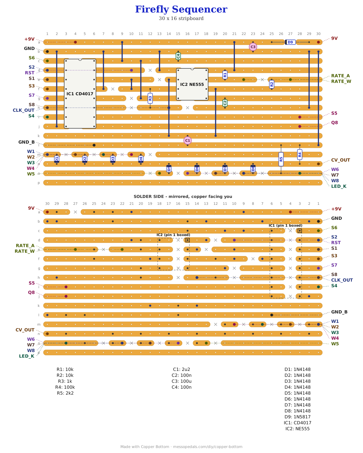
What you'll need
tap to expand / collapse
- 1× CD4017 decade counter, 16-pin DIP - spot it: CD4017 or HEF4017 printed on top, notch marks pin 1. The sixteen-pin one, not a 4022
- 1× NE555 timer, 8-pin DIP - spot it: 555 in the part number, notch or dot marks pin 1
- 8× 1N4148 signal diodes - spot it: tiny glass body, a black band at the cathode end. One per step, and they all stand up
- 1× 1N5817 Schottky - spot it: black body, a silver band. Reverse-polarity protection on the supply; a 1N4001 works too and costs half a volt
- 2× 10K (brown-black-orange) - the clock's upper timing resistor and the rate pot's floor
- 1× 1K (brown-black-red) on the clock output, 1× 100K (brown-black-yellow) holding the CV bus down, 1× 2K2 (red-red-red) - the one resistor all eight LEDs share
- 1× 2.2 µF electrolytic - the clock's timing cap. Spot it: the stripe marks the negative leg. A 1 µF runs twice as fast, a 4.7 half as fast
- 1× 100 µF electrolytic across the supply
- 2× 100n ceramic (104) - one on the 555's control pin, one across the 4017's supply pins
- 1× stripboard, 16 strips × 30 holes or larger, and wire for eleven links
Off the board
- 8× 100K linear pots (B100K) - the steps. All three lugs are used; see the wiring table
- 1× 1M linear pot (B1M) - the rate. Two lugs
- 8× LEDs, any color, 5 mm - one per step. They share one resistor, so make them the same color or the brightness will wander step to step
- 2× 3.5 mm jacks - CV out and clock out
- 1× DC jack or 9V battery snap, and a toggle for power if you want one
- A short wire from the Q8 pad to the RST pad, or a toggle in its place - see the step-count section
- A 1590BB box, lying flat - the drill template further down
The layout file is the guide
Like the 555 theremin and the Opto Duet, the build document for this one is the file itself: ↓ Download Firefly_Sequencer.json - import it into Copper Bottom and the editor gives you the board picture, the placement walkthrough, the electrical checks and a printable build sheet, all from the same file. No coordinates are written out on this page on purpose: the editor is the viewer, and a number typed twice is a number that can drift.
The netlist
Quoted verbatim from the layout file. It was written from the board, so checking the board against it can only pass - what it is for is carrying the circuit somewhere else, and telling you what each strip is supposed to be doing while you stare at it.
The off-board wiring
Twenty-nine pads leave the board, which sounds like a lot until you notice that twenty-four of them are the same three wires eight times over.
| Pad | Goes to |
|---|---|
| 9V / GND | The supply, 9V. GND_B is a second ground pad on the same net, there because a lot of things want to reach ground |
| S1 … S8 | Each step pot's lug 3, and that step's LED anode. Both on the same pad. Lug 1 of every step pot goes to GND |
| W1 … W8 | Each step pot's wiper. S1 pairs with W1, S2 with W2, and so on. Get a pair crossed and one knob sets the wrong step, which you will hear |
| LED_K | All eight LED cathodes, tied together. Only one step is ever high, so one resistor on the board serves all eight |
| RATE_A / RATE_W | The rate pot: one outer lug and the wiper. Tie the unused lug to the wiper so the knob cannot go open |
| Q8 / RST | A wire between them, for eight steps. See below for fewer |
| CV_OUT | Jack tip. The sequence, 0 to about 8V. Sleeve to GND |
| CLK_OUT | Jack tip. The clock, a 9V square wave through 1K - a gate or a trigger for whatever wants one. Sleeve to GND |
| +9V | Nothing. A test point on the protected rail, and it tells Copper Bottom's checker that strip is a supply |
The step pots are dividers, not variable resistors. Lug 3 to the S pad, lug 1 to ground, wiper to the W pad. Wired that way a knob turned fully down gives a real zero, and the diode on the board keeps that step's pot from loading the bus while another step is playing.
How many steps
The 4017 counts to ten. It loops at eight because Q8, the ninth count, is wired back to RST, so the moment the count reaches nine it snaps back to zero. Both come out on pads instead of being linked on the board, and that is the whole trick: wire Q8 to RST and you have eight steps; wire S5 to RST instead and you have four; S7 gives six. A toggle between Q8 and S5 on the RST pad is the classic mod, and it is free. Never wire two of them to RST at once - they are both outputs and they will fight.
How it works, in one breath
The 555 runs as an astable, the plain datasheet circuit: 10K up top, the rate pot plus a 10K floor in the middle, 2.2 µF to ground. With those values it ticks between about a third of a step a second and twenty a second. Every rising edge advances the 4017 one count, and the 4017 does the one thing it does: exactly one of its outputs is high at any moment and the rest are at ground.
The high output pushes 9V into the top of its step's pot and lights its LED. The pot divides that down to wherever the knob is, and the wiper sends it through a diode onto the CV bus, where a 100K holds it at zero between steps. The seven idle pots have their tops at ground, so their diodes are reverse-biased and they do not load the bus. The diode costs about half a volt, so the bus runs from zero to a little over 8V rather than the full nine.
Two things a builder should expect, unmeasured. The LED shares its output with the pot, so it pulls that output down a little under load - every step sags by the same amount, so the scale shifts as a whole and no step is wrong relative to another. And pins 11 and 12 of the 4017, Q9 and CARRY, go nowhere on purpose: they are outputs, and an unused CMOS output is happy floating. Copper Bottom lists them as orphans, and it is right that they are.
Playing the Dragonfly with it, untested: the Dragonfly's pitch pot is a divider into the 4046's VCO input, pin 9. Feeding CV_OUT to that node through a 100K, with the pitch pot left in as an offset, is how I would start. The clock out into anything with a gate input is the other half.
Print at 100% / “Actual size”, never “Fit to page” - check the bar measures exactly 4″ before you touch a drill. The dashed line is the 8 mm keep-out for the lid lip and the corner bosses.
Nobody has drilled this one yet. The hole sizes are the usual ones for these parts; where they sit is a proposal. Offer the sheet up to the box and check it against your own knobs before you make a hole.
Circuit from the CD4017 and NE555 datasheets' application notes - a 555 astable into a decade counter is the oldest sequencer there is. The step pots as dividers with the diodes on the wipers, the shared LED resistor, the reset on pads, the layout and the box are Onion Madder's, drawn in Copper Bottom.