Dragonfly VCO PCB v1.1
CD4046 on a 56 by 58 mm printed board, marked DRAGONFLY VCO v1.1 · By Onion Madder · Mess O' Pedals
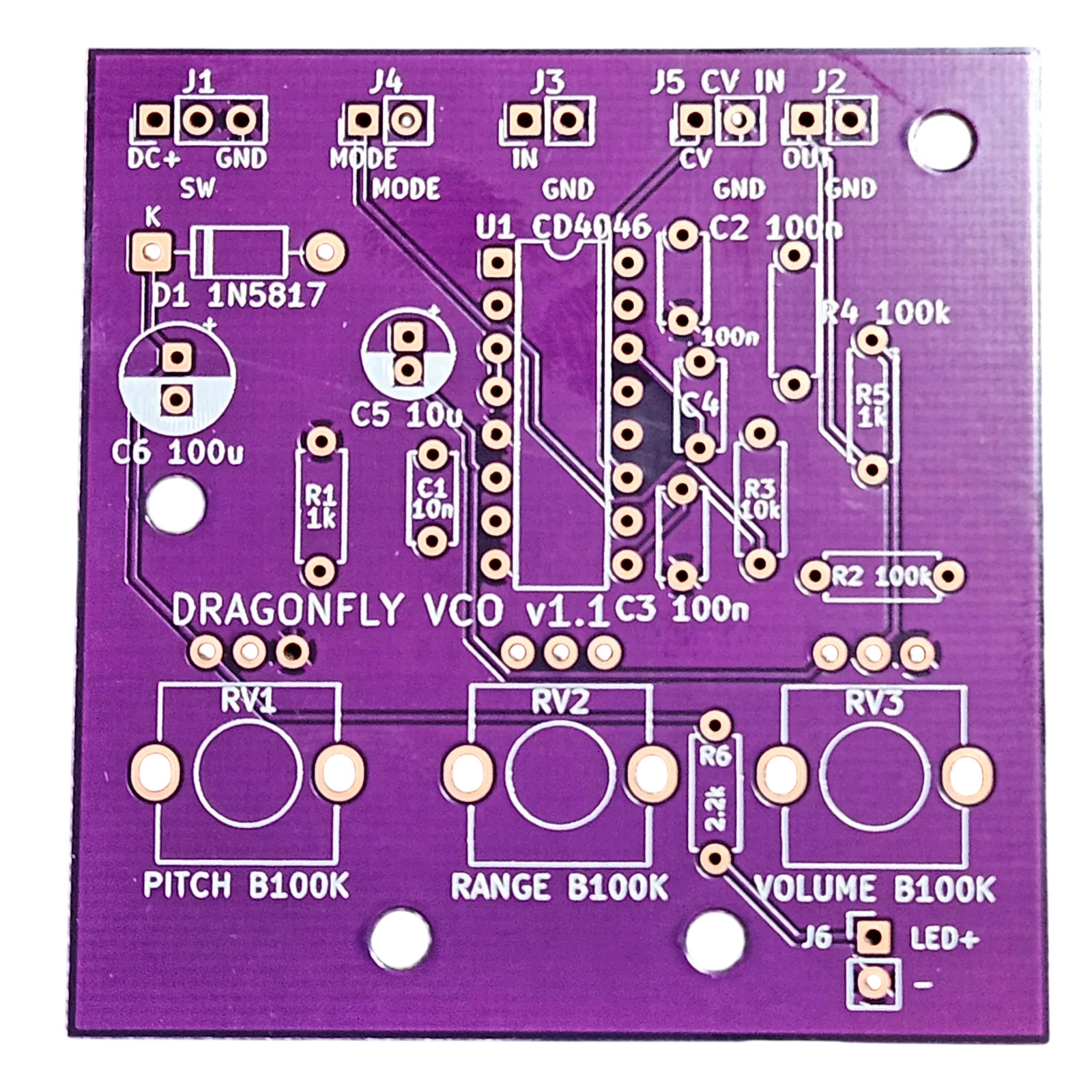
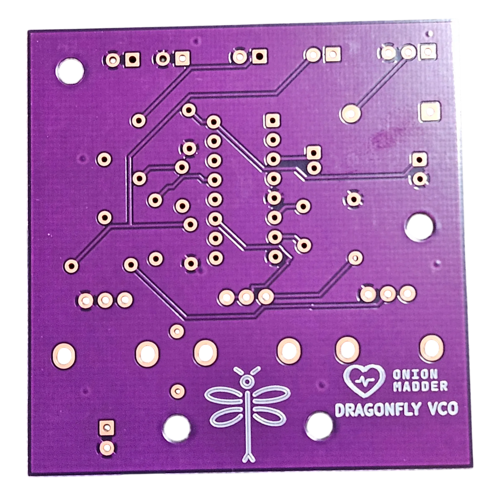
The Dragonfly VCO on its v1.1 board. A CD4046 phase-locked loop used as a plain, well-behaved oscillator, with PITCH, RANGE and VOLUME on the board, an input and a mode switch that let the loop chase whatever you feed it, and now a CV input with a header of its own.
What you'll need
tap to expand / collapse
17 parts on the board. The numbers in brackets are the ones printed on the board, and so is each part's value. ↓ Download the parts list (PDF), one page to print for the bench and tick off as each part goes in.
- 1× CD4046 (U1) - spot it: CD4046 printed on top, a notch or dot marks pin 1. The phase-locked loop. Pin 15, its zener, is left open on purpose
- 2× 100K resistor (R2, R4) - spot it: bands brown-black-yellow. R2 takes PITCH into pin 9; R4 is on the input
- 1× 10K resistor (R3) - spot it: bands brown-black-orange. From the phase comparator to the MODE switch
- 2× 1K resistor (R1, R5) - spot it: bands brown-black-red. R1 is the floor under RANGE; R5 is on the output
- 1× 10nF ceramic (C1) - spot it: printed 103. The VCO's timing cap, the thing that sets its range. Bigger means lower
- 3× 100nF ceramic (C2, C3, C4) - spot it: printed 104. Supply decoupling and two in the control path
- 1× 10 µF electrolytic (C5) - spot it: a can with a stripe down the minus leg. The long leg goes in the square pad, marked +. The output DC blocker
- 1× 100 µF electrolytic (C6) - spot it: a can with a stripe down the minus leg. The long leg goes in the square pad, marked +. Across the supply
- 1× 1N5817 (D1) - spot it: black body, gray band. The band goes to the square pad, the end the board marks with a band and a K. Reverse-polarity protection on the supply
- 1× 2.2K resistor (R6) - spot it: bands red-red-red. The power light's resistor
- 1× B100K pot, 9 mm, a Bourns PTV09A-4020F-B104 (RV1) - PITCH. Spot it: the B is the linear taper.
- 1× B100K pot, 9 mm, a Bourns PTV09A-4020F-B104 (RV2) - RANGE. Spot it: the B is the linear taper.
- 1× B100K pot, 9 mm, a Bourns PTV09A-4020F-B104 (RV3) - VOLUME. Spot it: the B is the linear taper.
- 1× Dragonfly VCO PCB v1.1
Off the board
- 1× DC jack and a 9V supply, center negative
- 1× SPST toggle for power, between the DC jack's + lug and SW
- 1× LED for power, on J6, if you want one
- 1× SPST toggle for the mode, across the two MODE pins
- 2× 3.5 mm mono jacks: the input, on IN, and the output, on OUT
- 1× 3.5 mm mono jack for CV, on CV IN, if you want it
- Hookup wire
What changed from v1.0
- CV IN has its own header, J5. On v1.0 a sequencer would not play through IN, because IN goes through a capacitor that blocks steady steps, and the fix was a wire to RANGE's middle leg on the back of the board. That wire is now J5: CV goes to RANGE's middle leg, pin 11, the current that sets the oscillator's pitch. On my v1.0 board that wiring played a sequencer, and RANGE set how far apart the notes were.
- IN is still there, J3, through R4 and C4 to pin 14, for audio the loop chases with MODE closed. Fit either jack, or both.
- A power light header, J6. Its resistor, R6, 2.2K, is on the board. On v1.0 the light and its resistor were wired off the board.
- The pots are 9 mm Bourns PTV09A-4s (PITCH, RANGE and VOLUME), still soldered to the board, in place of v1.0's 16 mm pots.
- The ceramic caps' holes are 5.08 mm apart, not 2.5, so a dipped ceramic drops in flat with no leg to kink.
- Every value is printed on the board, on the part's outline or beside it, with its number.
- Four M3 mounting holes. These pots have no nut, so they do not hold the board to the face the way v1.0's did. The holes are for standoffs or screws.
The headers
Everything that leaves the board leaves from a header, and each one has its pins labeled on the board. The square pad is pin 1, the first one named here.
| Header | Pins | Goes to |
|---|---|---|
| J1 | DC+ / SW / GND | Power, wired the usual way: the DC jack's + lug to one lug of the power toggle, the toggle's other lug to SW, and the jack's - lug to GND. On a center-negative supply the + is the jack's sleeve lug and the - is its center pin. SW is the board's power input, through D1, which guards against a supply plugged in the wrong way around. DC+ connects to nothing on the board: it is a spare pad to join the jack's + and the toggle on, if that is easier, and it can stay empty |
| J4 | MODE / MODE | The mode toggle, across the two pins. Closed, the loop chases the input instead of sitting where PITCH put it |
| J3 | IN / GND | The audio input jack: tip to IN, sleeve to GND. The loop's signal input, which it chases with MODE closed |
| J5 CV IN | CV / GND | The CV input jack: tip to CV, sleeve to GND. This is the one for a sequencer |
| J2 | OUT / GND | The output jack: tip to OUT, sleeve to GND |
| J6 | LED+ / - | The power light, if you want one: the LED's long leg to LED+ and its short leg to -. Its resistor, R6, 2.2K, is on the board. It lights when the power toggle is on |
Building it
- Lowest parts first, so the board sits flat on the bench while you solder: resistors, then the diodes, then the small ceramic caps.
- Before any chip goes in, power it up once. Fit the DC jack and the power toggle on their header, switch on, and put the meter's black probe on a GND pin and the red one in U1's pin 16 hole, from the top. You want the supply, less about 0.2V for the diode. Nothing there, or the full supply with the leads reversed, means look at the diode's band before going on. Switch off.
- The chips (U1), soldered straight in. Pin 1 goes to the square pad, the end the board marks with a notch.
- The electrolytics, long leg in the square pad, marked +.
- The pots last. Each one's three legs go in the three round holes and its two side tabs in the two slots. Seat it flat on the board with its shaft square, then solder the legs and both tabs; a crooked pot is a hole that will not line up.
- Fixing it in the box. These pots have no nut, so they do not hold the board to the face. The four holes in the board are for M3 standoffs: screwed through the face, or the stick-on kind.
- The headers. Wire them to the jacks and switches in the table above.
The board's four M3 holes are on the sheet as small dashed circles. They are optional: screws through the face into standoffs, or stick-on standoffs and no holes at all.
Print at 100% / “Actual size”, never “Fit to page”, and check the bar measures exactly 4″ before you touch a drill.
Nobody has drilled this one yet, and how far the board sits behind the face is not measured: your standoffs set it. Offer the sheet up to your own box, board and parts before you make a hole.
The circuit and every part value are the Dragonfly VCO PCB's, the v1.0 board. Board by Onion Madder.